鈩?/div>
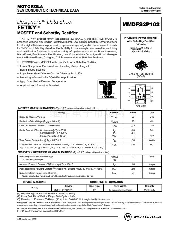
A
S
G
MOSFET MAXIMUM RATINGS
(TJ = 25擄C unless otherwise noted) (1)
Rating
Drain鈥搕o鈥揝ource Voltage
Drain鈥搕o鈥揋ate Voltage (RGS = 1.0 M
W
)
Gate鈥搕o鈥揝ource Voltage 鈥?Continuous
Drain Current (3) 鈥?Continuous @ TA = 25擄C
鈥?Continuous @ TA = 100擄C
鈥?Single Pulse (tp
10
m
s)
Symbol
VDSS
VDGR
VGS
ID
ID
IDM
PD
EAS
Value
20
TOP VIEW
Unit
Vdc
Vdc
Vdc
Adc
Apk
Watts
mJ
"
20
3.3
2.1
20
2.0
324
20
v
Total Power Dissipation @ TA = 25擄C (2)
Single Pulse Drain鈥搕o鈥揝ource Avalanche Energy 鈥?STARTING TJ = 25擄C
VDD = 30 Vdc, VGS = 5.0 Vdc, VDS = 20 Vdc, IL = 9.0 Apk, L = 10 mH, RG = 25
W
SCHOTTKY RECTIFIER MAXIMUM RATINGS
(TJ = 25擄C unless otherwise noted)
Peak Repetitive Reverse Voltage
DC Blocking Voltage
Average Forward Current (3) (Rated VR) TA = 100擄C
Peak Repetitive Forward Current (3) (Rated VR, Square Wave, 20 kHz) TA = 105擄C
Non鈥揜epetitive Peak Surge Current
(Surge applied at rated load conditions, halfwave, single phase, 60 Hz)
VRRM
VR
IO
Ifrm
Ifsm
20
1.0
2.0
20
Volts
Amps
Amps
Amps
DEVICE MARKING
2P102
Device
MMDFS2P102R2
ORDERING INFORMATION
Reel Size
13鈥?/div>
Tape Width
12 mm embossed tape
Quantity
2500 units
(1) Negative sign for P鈥揷hannel device omitted for clarity.
(2) Pulse Test: Pulse Width
鈮?/div>
250
碌s,
Duty Cycle
鈮?/div>
2.0%.
(3) Mounted on 2鈥?square FR4 board (1鈥?sq. 2 oz. Cu 0.06鈥?thick single sided), 10 sec. max.
Designer鈥檚 Data for 鈥淲orst Case鈥?Conditions
鈥?The Designer鈥檚 Data Sheet permits the design of most circuits entirely from the information presented. SOA Limit
curves 鈥?representing boundaries on device characteristics 鈥?are given to facilitate 鈥渨orst case鈥?design.
HDTMOS and Designer鈥檚 are trademarks of Motorola, Inc. TMOS is a registered trademark of Motorola, Inc.
FETKY is a trademark of International Rectifier.
漏
Motorola TMOS
Motorola, Inc. 1997
Product Preview Data
1


 1
1
 2
2
 3
3
 4
4
 5
5
 6
6
 7
7
 8
8
 9
9
 10
10
 11
11
 12
12
