鈥?/div>
Standard Pinouts 鈥?No Additional Pins or Components Required
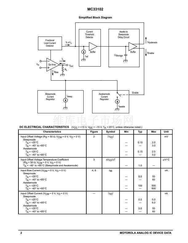
Sleepmode State 鈥?Can Be Used in the Low Current Idle State as a
Fully Functional Micropower Amplifier
Automatic Return to Sleepmode when Output Current Drops Below
Threshold
No Deadband/Crossover Distortion; as Low as 1.0 Hz in the Awakemode
Drop鈥搃n Replacement for Many Other Dual Op Amps
ESD Clamps on Inputs Increase Reliability without Affecting Device
Operation
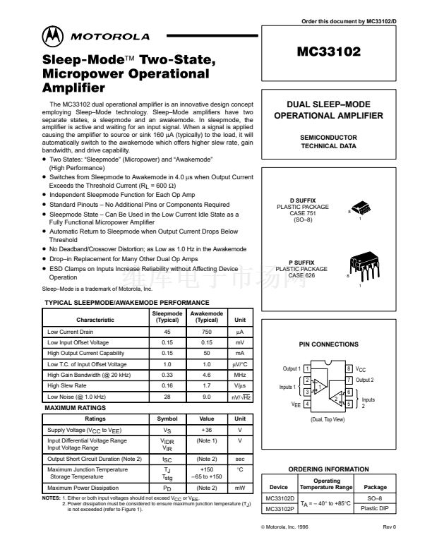
D SUFFIX
PLASTIC PACKAGE
CASE 751
(SO鈥?)
8
1
P SUFFIX
PLASTIC PACKAGE
CASE 626
8
1
Sleep鈥揗ode is a trademark of Motorola, Inc.
TYPICAL SLEEPMODE/AWAKEMODE PERFORMANCE
Characteristic
Low Current Drain
Low Input Offset Voltage
High Output Current Capability
Low T.C. of Input Offset Voltage
High Gain Bandwidth (@ 20 kHz)
High Slew Rate
Low Noise (@ 1.0 kHz)
Sleepmode
(Typical)
45
0.15
0.15
1.0
0.33
0.16
28
Awakemode
(Typical)
750
0.15
50
1.0
4.6
1.7
9.0
Unit
碌A(chǔ)
mV
mA
碌V/擄C
MHz
V/碌s
nV/
鈭?/div>
Hz
Inputs 1
Output 1 1
2
3
1
2
8
7
6
5
Inputs
2
VCC
Output 2
PIN CONNECTIONS
MAXIMUM RATINGS
Ratings
Supply Voltage (VCC to VEE)
Input Differential Voltage Range
Input Voltage Range
Output Short Circuit Duration (Note 2)
Maximum Junction Temperature
Storage Temperature
Maximum Power Dissipation
Symbol
VS
VIDR
VIR
tSC
TJ
Tstg
PD
Value
+ 36
(Note 1)
(Note 2)
+150
鈥?65 to +150
(Note 2)
Unit
V
V
sec
擄C
mW
Device
VEE 4
(Dual, Top View)
ORDERING INFORMATION
Operating
Temperature Range
TA = 鈥?40擄 to +85擄C
Package
SO鈥?
Plastic DIP
NOTES:
1. Either or both input voltages should not exceed VCC or VEE.
2. Power dissipation must be considered to ensure maximum junction temperature (TJ)
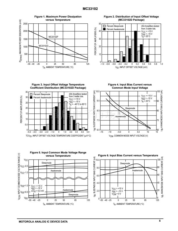
is not exceeded (refer to Figure 1).
MC33102D
MC33102P
漏
Motorola, Inc. 1996
Rev 0
MOTOROLA ANALOG IC DEVICE DATA
1


 1
1
 2
2
 3
3
 4
4
 5
5
 6
6
 7
7
 8
8
 9
9
 10
10
 11
11
 12
12
 13
13
 14
14
