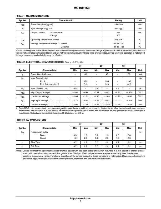
鈥?/div>
Pb鈭扚ree Packages are Available*
16
16
1
Q
L
H
L
H
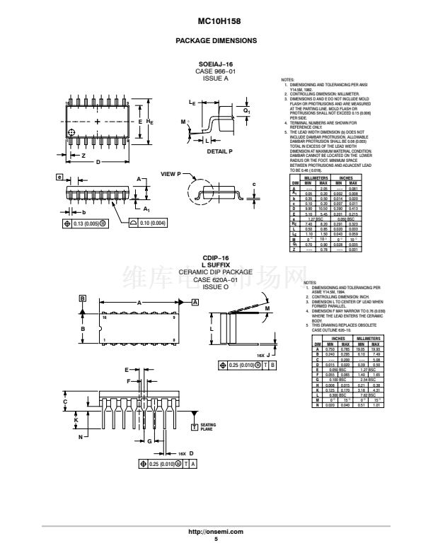
SOEIAJ鈭?6
CASE 966
1 20
V
CC
Q2
Q3
D20
D21
D30
D31
SELECT
20 1
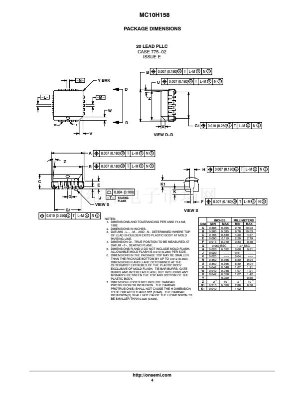
PLLC鈭?0
FN SUFFIX
CASE 775
A
WL, L
YY, Y
WW, W
G
= Assembly Location
= Wafer Lot
= Year
= Work Week
= Pb鈭扚ree Package
10H158G
AWLYYWW
10H158
ALYWG
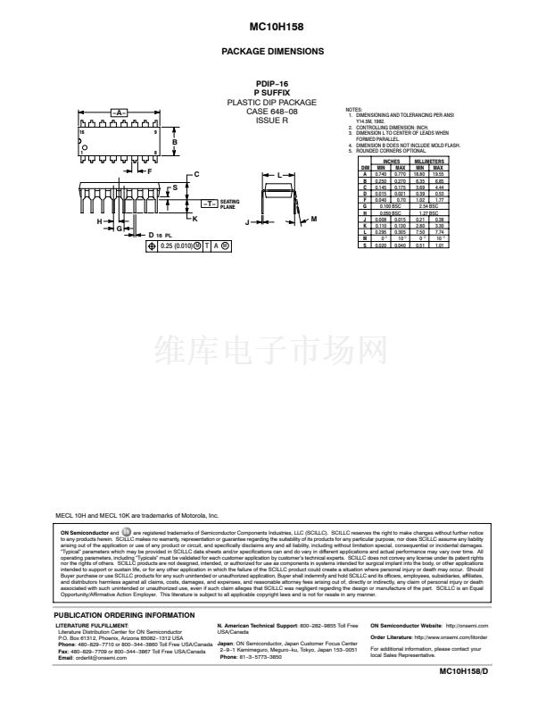
PDIP鈭?6
P SUFFIX
CASE 648
1
MC10H158P
AWLYYWWG
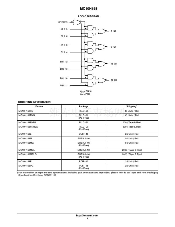
TRUTH TABLE
Select
L
L
H
H
D0
X
X
L
H
D1
L
H
X
X
DIP
PIN ASSIGNMENT
Q0
Q1
D11
D10
D01
D00
NC
V
EE
1
2
3
4
5
6
7
8
16
15
14
13
12
11
10
9
Pin assignment is for Dual鈭抜n鈭扡ine Package.
For PLCC pin assignment, see the Pin Conversion Tables on page 18
of the ON Semiconductor MECL Data Book (DL122/D).
*For additional marking information, refer to
Application Note AND8002/D.
*For additional information on our Pb鈭扚ree strategy and soldering details, please
download the ON Semiconductor Soldering and Mounting Techniques
Reference Manual, SOLDERRM/D.
ORDERING INFORMATION
See detailed ordering and shipping information in the package
dimensions section on page 3 of this data sheet.
漏
Semiconductor Components Industries, LLC, 2006
February, 2006
鈭?/div>
Rev. 7
1
Publication Order Number:
MC10H158/D


 1
1
 2
2
 3
3
 4
4
 5
5
 6
6
