19-2486; Rev 0; 7/02
+14dBm to +20dBm LO Buffers
with 鹵1dB Variation
General Description
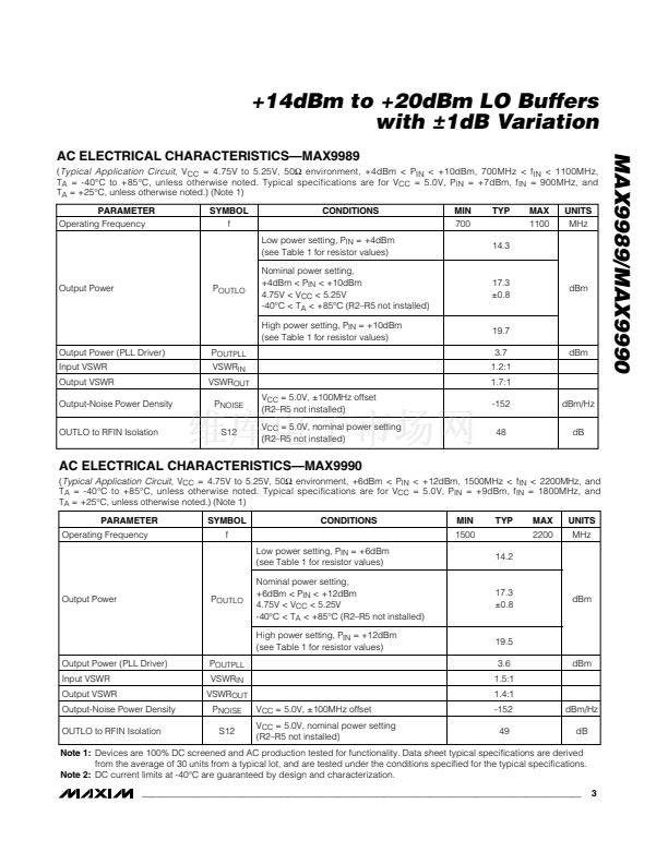
The MAX9989 and MAX9990 LO buffers provide the high
output (+14dBm to +20dBm) necessary to drive the LO
inputs of high-linearity passive mixers, while offering 40dB
reverse isolation to prevent LO pulling. The MAX9989 is
internally matched for the cellular/GSM bands, and the
MAX9990 is matched for the DCS/PCS/UMTS bands.
The
Typical Application Circuit
provides a nominal
+17dBm output power with 鹵1dB variation over supply,
temperature, and input power. With two optional resis-
tors, the output power can be precision set from
+14dBm to +20dBm. The devices offer more than 35dB
main driver output to PLL amp output isolation. Each
device is offered in a 5mm
鉁?/div>
5mm 20-pin thin QFN
package with exposed paddle.
o
鹵1dB Output Power Variation
o
+14dBm to +20dBm Adjustable Output Power
o
40dB Reverse Isolation
o
Better Than 35dB Main Driver Output to PLL Amp
Output Isolation
o
Low Output Noise: -170dBc/Hz at +17dBm
o
110mA Supply Current at +17dBm
o
ESD Protection
o
Isolated PLL Output (+3dBm)
Features
MAX9989/MAX9990
Applications
Cellular/GSM/DCS/PCS/UMTS Base Station
Tx/Rx LO Drives
Coherent Receivers
ISM Wireless LAN
Wireless Local Loop
Local Multipoint Distribution Service
Point-to-Point Systems
PART
Ordering Information
TEMP
RANGE
PIN-
PACKAGE
20 Thin
QFN-EP*
FREQUENCY
RANGE (MHz)
700 to 1100
MAX9989ETP
-40擄C to +85擄C
MAX9990ETP
-40擄C to +85擄C 20 QFN-EP* 1500 to 2200
*EP =
Exposed paddle.
Typical Application Circuit/Pin Configuration appears at end of data sheet.
Typical Operating Circuit and Block Diagram
PLL BUFFER
TO PLL
PRESCALER
OUTPLL
(+3dBm)
MAX9989
MAX9990
OUTPUT AMP
INPUT AMP
RF INPUT
IN
(+7dBm)
RF LO
OUTLO
(+17dBm)
IF OUTPUT
BIAS
BIASIN
BIASOUT
BIAS
CONTROL
NETWORK
________________________________________________________________
Maxim Integrated Products
1
For pricing, delivery, and ordering information, please contact Maxim/Dallas Direct! at
1-888-629-4642, or visit Maxim鈥檚 website at www.maxim-ic.com.


 1
1
 2
2
 3
3
 4
4
 5
5
 6
6
 7
7
 8
8
 9
9
 10
10
 11
11
 12
12
