19-1417; Rev 0; 12/98
MAX3693 Evaluation Kit
General Description
The MAX3693 evaluation kit (EV kit) is an assembled,
surface-mount demonstration board that provides easy
evaluation of the MAX3693 622Mbps serializer with
clock synthesis and LVDS inputs.
o
Single +3.3V Supply
o
Selectable Clock-Reference Frequencies
(155.52MHz, 77.76MHz, 51.84MHz, 38.88MHz)
o
Fully Assembled and Tested Surface-Mount
Board
Features
Evaluates: MAX3693
Component List
DESIGNATION QTY
C4鈥揅9, C11,
C12, C16鈥揅21
C13, C22
C14
C15
L1鈥揕5
R1, R2, R11,
C1鈥揅3, C10,
JU1, JU2, JU4,
JU11鈥揓U15
R3, R4
R5, R6
R7, R8
R9, R10
R12
PCLKI+,
PCLKI-, PD0+,
PD0-, PD1+,
PD1-, PD2+,
PD2-, PD3+,
PD3-, PCLK0+,
PCLK0-
RCLK+, RCLK-,
SD+, SD-
GND, +3.3V
JU3
U1
14
2
1
1
1
DESCRIPTION
0.1碌F, 10%, 25V min ceramic
capacitors
1碌F, 10%, 10V min ceramic
capacitors X7R type
1碌F, 10%, 25V min ceramic capacitor
33碌F, 鹵10%, 10V min tantalum
capacitor AVX TAJD336K010
56nH inductors
Coilcraft 0805CS-560XKBC
Not installed
27鈩? 5% resistors
220鈩? 5% resistors
130鈩? 5% resistors
24鈩? 5% resistors
20k鈩? 5% resistor
Ordering Information
PART
MAX3693EVKIT
TEMP. RANGE
-40擄C to +85擄C
IC PACKAGE
32 TQFP
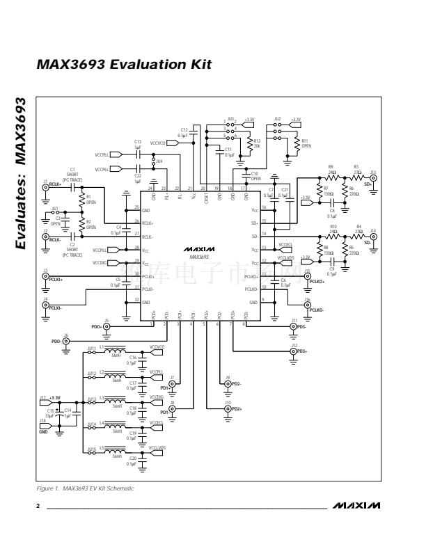
Detailed Description
The MAX3693 EV kit simplifies evaluation of the
MAX3693. The EV kit operates from a single +3.3V supply
and includes all the external components necessary to
interface with LVDS inputs and 3.3V PECL outputs.
The LVDS inputs (PD_+, PD_-, PCLKI+, PCLKI-,
RCLK+, RCLK-) are internally terminated with 100鈩?dif-
ferential input resistance, and therefore do not require
external termination. Ensure that LVDS devices driving
these inputs are not redundantly terminated. The LVDS
outputs (PCLKO+, PCLKO-) require a differential termi-
nation with a 100鈩?resistor between complementary
outputs.
The evaluation kit is designed to directly couple an
LVDS reference clock. If the reference clock does not
have LVDS-compatible levels:
1) Cut the PC board traces shorting capacitors C1
and C2.
2) Install 0.1碌F capacitors.
3) Install 4.99k鈩?resistors for R1 and R2 and tie the
centerpoint of R1 and R2 (available at JU1) to
V
CC
/ 2. Install a 0.1碌F capacitor at C3 for add-
tional noise filtering.
The PECL outputs have an attenuation (0.6) and imped-
ance matching network on the EV board that allow 50鈩?/div>
terminations to ground for oscilloscope interfacing. All
signal inputs and outputs use coupled 50鈩?transmis-
sion lines. All input signal lines are of equal length to
minimize propagation-delay skew. Likewise, all output
signal lines are of equal length.
The MAX3693 EV kit allows use of multiple reference
clock frequencies with the appropriate setting on JU3.
See Table 1 for jumper settings.
1
0
2
2
2
2
1
12
SMB connectors (PC-mount)
4
2
1
1
1
1
1
SMA connectors (PC-mount)
Test points
2x3 pin header
MAX3693ECJ (32 TQFP)
MAX3693 PC board
MAX3693 data sheet
Shunt for JU3
Component Suppliers
SUPPLIER
AVX
Coilcraft
PHONE
803-946-0690
847-639-6400
FAX
803-626-3123
847-639-1469
________________________________________________________________
Maxim Integrated Products
For free samples & the latest literature: http://www.maxim-ic.com, or phone 1-800-998-8800.
For small orders, phone 1-800-835-8769.


 1
1
 2
2
 3
3
 4
4
