鈻?/div>
Input Voltage Range:
1.14V to 3.5V (with Boost Enabled)
1.14V to 5.5V (with External 5V Boost)
Low Dropout Voltage: 100mV at I
OUT
= 1.5A
Adjustable Output Range: 0.4V to 2.6V
Output Current: Up to 1.5A
Excellent Supply Rejection Even Near Dropout
Shutdown Disconnects Load from V
IN
and V
BST
Low Operating Current: I
IN
= 950碌A at V
IN
= 1.5V
Low Shutdown Current:
I
IN
< 1碌A (Typ), I
BST
= 0.1碌A (Typ)
Stable with 10碌F or Greater Ceramic Capacitors
Short-Circuit, Reverse Current Protected
Overtemperature Protected
Available in 10-Lead MSOP and 10-Lead
(3mm
脳
3mm) DFN Packages
The LTC
廬
3026 is a very low dropout (VLDO
TM
) linear
regulator that can operate at input voltages down to 1.14V.
The device is capable of supplying 1.5A of output current
with a typical dropout voltage of only 100mV. To allow
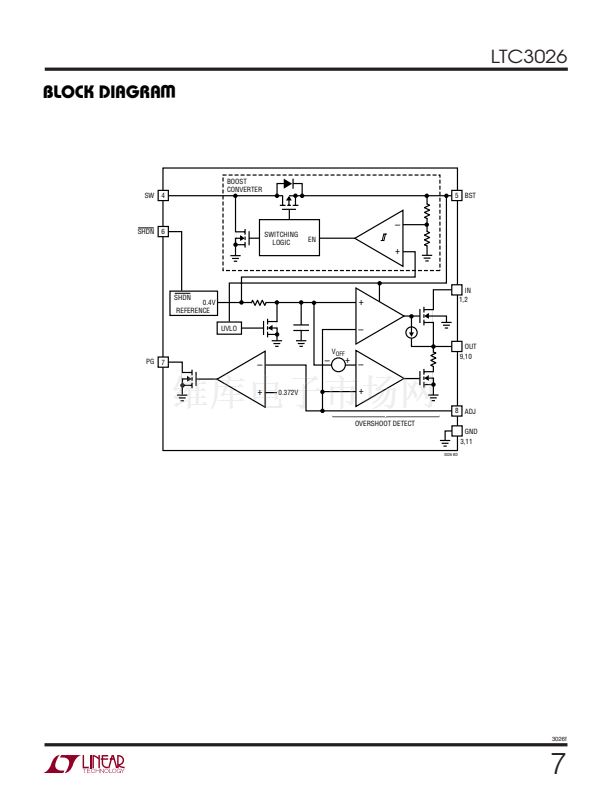
operation at low input voltages the LTC3026 includes a
boost converter that provides the necessary headroom for
the internal LDO circuitry.
Output current comes directly from the input supply to
maximize efficiency. The boost converter requires only a
small chip inductor and ceramic capacitor for operation.
Additionally, the boosted output voltage of one LTC3026
can supply the boost voltage for other LTC3026s, thus
requiring a single inductor for multiple LDOs. A user
supplied boost voltage can be used eliminating the need
for an inductor altogether.
The LTC3026 regulator is stable with 10碌F or greater
ceramic output capacitors. The device has a low 0.4V
reference voltage which is used to program the output
voltage via two external resistors. The device also has
internal current limit, overtemperature shutdown, and
reverse output current protection. The LTC3026 is avail-
able in a small 10-lead MSOP or low profile (0.75mm)
10-lead 3mm
脳
3mm DFN package.
APPLICATIO S
鈻?/div>
鈻?/div>
鈻?/div>
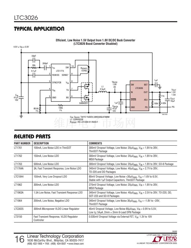
High Efficiency Linear Regulator
Post Regulator for Switching Supplies
Microprocessor Supply
, LTC and LT are registered trademarks of Linear Technology Corporation.
VLDO is a trademark of Linear Technology Corporation.
All other trademarks are the property of their respective owners.
Patent Pending
TYPICAL APPLICATIO
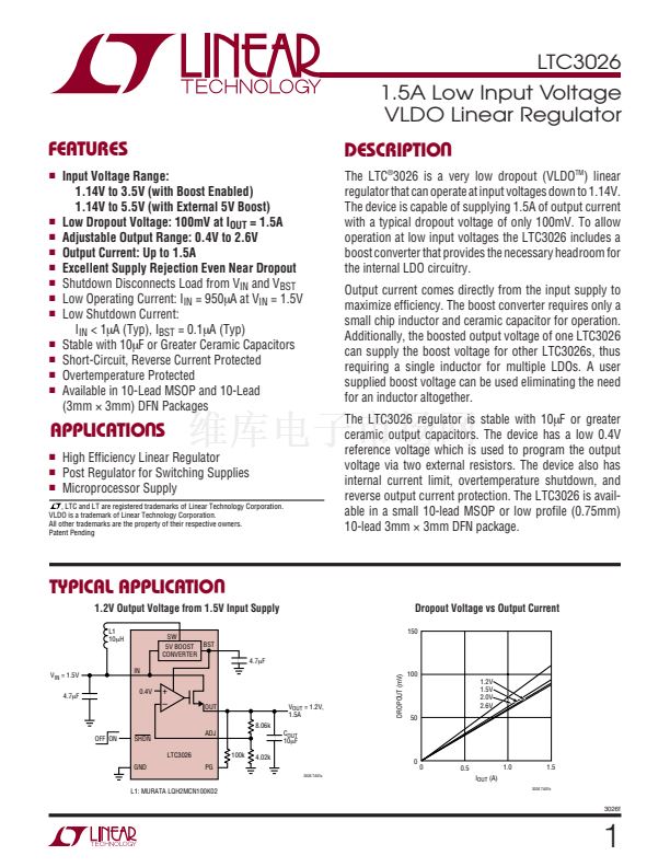
L1
10碌H
SW
1.2V Output Voltage from 1.5V Input Supply
5V BOOST BST
CONVERTER
IN
0.4V
Dropout Voltage vs Output Current
150
4.7碌F
DROPOUT (mV)
V
IN
= 1.5V
4.7碌F
100
1.2V
1.5V
2.0V
2.6V
50
+
鈥?/div>
OUT
8.06k
V
OUT
= 1.2V,
1.5A
C
OUT
10碌F
100k
4.02k
3026 TA01a
OFF ON
SHDN
LTC3026
GND
ADJ
PG
0
0
L1: MURATA LQH2MCN100K02
U
0.5
I
OUT
(A)
3026 TA01b
U
U
1.0
1.5
3026f
1


 1
1
 2
2
 3
3
 4
4
 5
5
 6
6
 7
7
 8
8
 9
9
 10
10
 11
11
 12
12
 13
13
 14
14
 15
15
 16
16
