鈥?/div>
Moisture Sensitivity Level: 1
http://onsemi.com
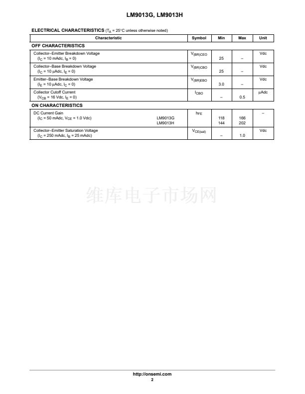
MAXIMUM RATINGS
Rating
Collector-Emitter Voltage
Collector-Base Voltage
Emitter-Base Voltage
Collector Current 鈥?Continuous
Total Device Dissipation
@ T
A
= 25擄C
Derate above 25擄C
Total Device Dissipation
@ T
C
= 25擄C
Derate above 25擄C
Operating and Storage Junction
Temperature Range
Symbol
V
CEO
V
CBO
V
EBO
I
C
P
D
625
5.0
P
D
1.5
12
T
J
, T
stg
鈥?5 to
+150
Watts
mW/擄C
擄C
1
mW
mW/擄C
Value
25
25
3.0
1000
Unit
Vdc
Vdc
Vdc
mAdc
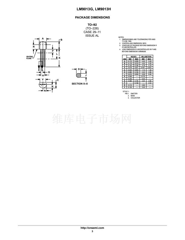
2
BASE
COLLECTOR
3
1
EMITTER
THERMAL CHARACTERISTICS
Characteristic
Thermal Resistance, (Note 1.)
Junction to Ambient
Thermal Resistance,
Junction to Case
Symbol
R
胃JA
R
胃JC
Max
200
83.3
Unit
擄C/W
擄C/W
2
3
TO鈥?2
CASE 29
STYLE 1
1. R
qJA
is measured with the device soldered into a typical printed circuit board.
LM90
13x
YWW
LM9013x = Specific Device Code
x
= G or H
Y
= Year
WW
= Work Week
ORDERING INFORMATION
Device
LM9013G
LM9013H
Package
TO鈥?2
TO鈥?2
Shipping
5000 Units/Box
5000 Units/Box
Preferred
devices are recommended choices for future use
and best overall value.
漏
Semiconductor Components Industries, LLC, 2001
1
April, 2001 鈥?Rev. 0
Publication Order Number:
LM9013G/D


 1
1
 2
2
 3
3
 4
4
