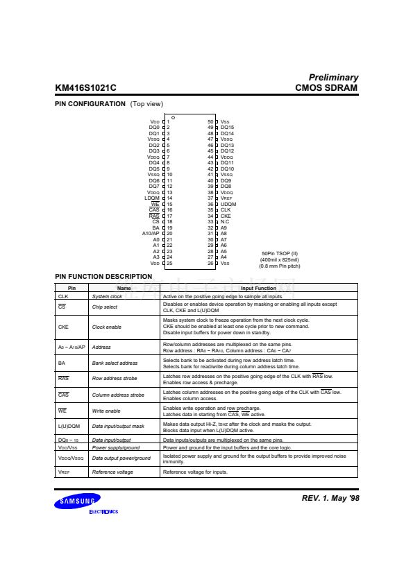
KM416S1021C
512K x 16Bit x 2 Banks Synchronous DRAM with SSTL interface
FEATURES
鈥?JEDEC standard 3.3V power supply
鈥?SSTL_3 (Class II) compatible with multiplexed address
鈥?Dual banks operation
鈥?MRS cycle with address key programs
- CAS latency (2 & 3)
- Burst length (1, 2, 4, 8 & Full page)
- Burst type (Sequential & Interleave)
鈥?All inputs are sampled at the positive going edge of the system
clock.
鈥?Burst read single-bit write operation
鈥?DQM for masking
鈥?Auto & self refresh
鈥?64ms refresh period (4K cycle)
Preliminary
CMOS SDRAM
GENERAL DESCRIPTION
The KM416S1021C is 16,777,216 bits synchronous high data
rate Dynamic RAM organized as 2 x 524,288 words by 16 bits,
fabricated with SAMSUNG鈥瞫 high performance CMOS technol-
ogy. Synchronous design allows precise cycle control with the
use of system clock I/O transactions are possible on every clock
cycle. Range of operating frequencies, programmable burst
length and programmable latencies allow the same device to be
useful for a variety of high bandwidth, high performance mem-
ory system applications.
ORDERING INFORMATION
Part No.
KM416S1021CT-G7
KM416S1021CT-GS
Max Freq.
143MHz
100MHz(CL=2)
Interface Package
SSTL_3
(Class II)
54
TSOP(II)
KM416S1021CT-G8
125MHz
* KM416S1021CT-GS : CL=2 only
FUNCTIONAL BLOCK DIAGRAM
I/O Control
LWE
Data Input Register
LDQM
Bank Select
Refresh Counter
Output Buffer
Row Decoder
Sense AMP
512K x 16
Row Buffer
DQi
Address Register
CLK
ADD
512K x 16
Column Decoder
Col. Buffer
Latency & Burst Length
LRAS
LCBR
LCKE
LRAS
LCBR
LWE
LCAS
Programming Register
LWCBR
LDQM
Timing Register
CLK
CKE
CS
RAS
CAS
WE
L(U)DQM
* Samsung Electronics reserves the right to
change products or specification without
notice.
REV. 1. May '98


 1
1
 2
2
 3
3
 4
4
 5
5
 6
6
 7
7
 8
8
