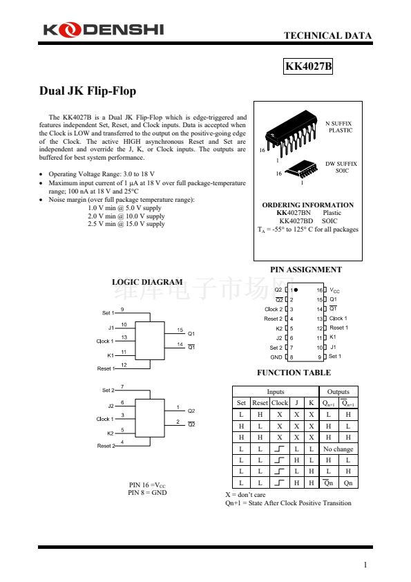
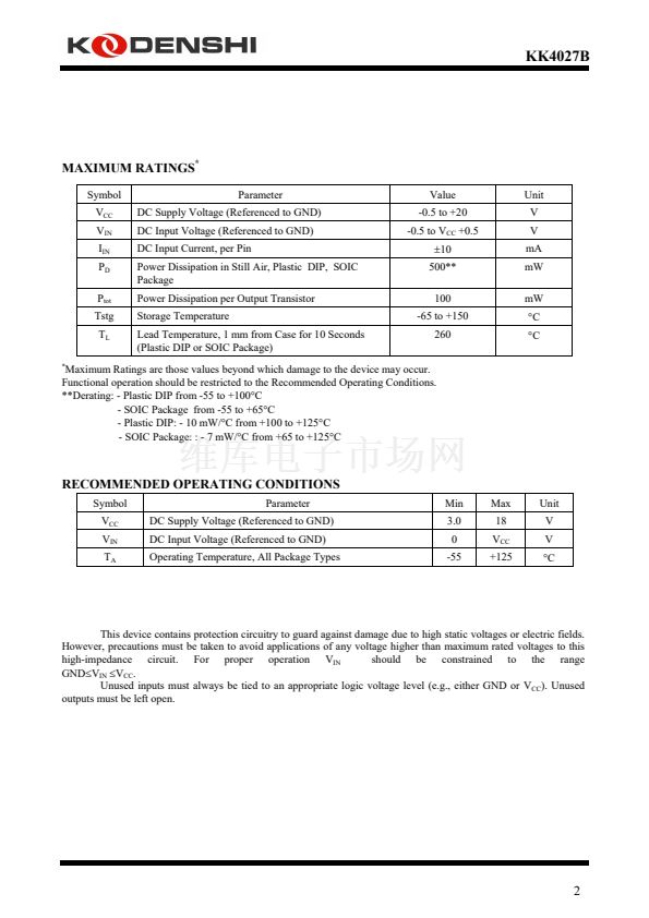
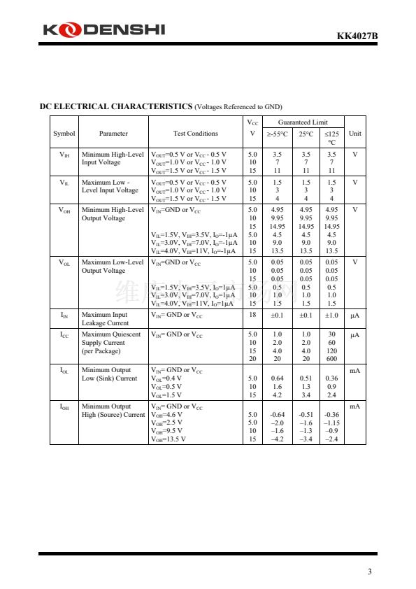
TECHNICAL DATA
KK4027B
Dual JK Flip-Flop
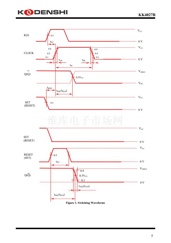
The KK4027B is a Dual JK Flip-Flop which is edge-triggered and
features independent Set, Reset, and Clock inputs. Data is accepted when
the Clock is LOW and transferred to the output on the positive-going edge
of the Clock. The active HIGH asynchronous Reset and Set are
independent and override the J, K, or Clock inputs. The outputs are
buffered for best system performance.
鈥?/div>
Operating Voltage Range: 3.0 to 18 V
鈥?/div>
Maximum input current of 1
碌A
at 18 V over full package-temperature
range; 100 nA at 18 V and 25擄C
鈥?/div>
Noise margin (over full package temperature range):
1.0 V min @ 5.0 V supply
2.0 V min @ 10.0 V supply
2.5 V min @ 15.0 V supply
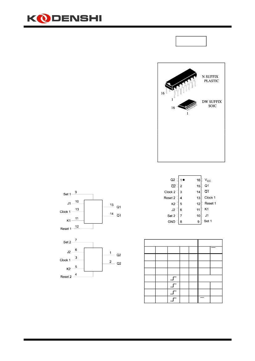
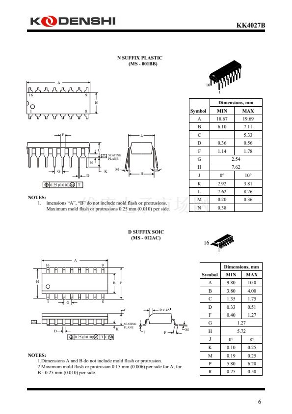
ORDERING INFORMATION
KK4027BN
Plastic
KK4027BD SOIC
T
A
= -55擄 to 125擄 C for all packages
PIN ASSIGNMENT
LOGIC DIAGRAM
FUNCTION TABLE
Inputs
Set Reset Clock
L
H
H
L
L
L
PIN 16 =V
CC
PIN 8 = GND
L
H
L
H
L
L
L
L
X
X
X
J
X
X
X
L
H
L
H
K
X
X
X
L
L
H
H
Outputs
Q
n+1
L
H
H
H
L
Qn
Q
n+1
H
L
H
L
H
Qn
No change
X = don鈥檛 care
Qn+1 = State After Clock Positive Transition
1


 1
1
 2
2
 3
3
 4
4
 5
5
 6
6
