K9F2808Q0C-DCB0,DIB0
K9F2808U0C-YCB0,YIB0
K9F2808U0C-DCB0,DIB0
K9F2816Q0C-DCB0,DIB0
K9F2816U0C-YCB0,YIB0
K9F2816U0C-DCB0,DIB0
K9F2808U0C-VCB0,VIB0
FLASH MEMORY
Document Title
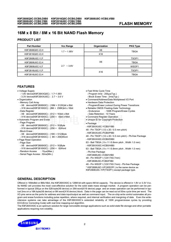
16M x 8 Bit , 8M x 16 Bit NAND Flash Memory
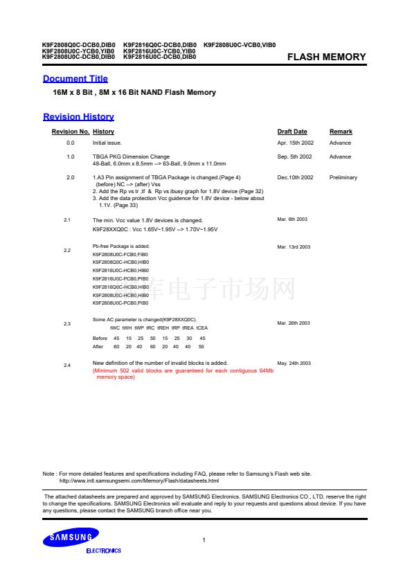
Revision History
Revision No. History
0.0
1.0
Initial issue.
TBGA PKG Dimension Change
48-Ball, 6.0mm x 8.5mm --> 63-Ball, 9.0mm x 11.0mm
1.A3 Pin assignment of TBGA Package is changed.(Page 4)
(before) NC --> (after) Vss
2. Add the Rp vs tr ,tf & Rp vs ibusy graph for 1.8V device (Page 32)
3. Add the data protection Vcc guidence for 1.8V device - below about
1.1V. (Page 33)
The min. Vcc value 1.8V devices is changed.
K9F28XXQ0C : Vcc 1.65V~1.95V --> 1.70V~1.95V
Pb-free Package is added.
K9F2808U0C-FCB0,FIB0
K9F2808Q0C-HCB0,HIB0
K9F2816U0C-HCB0,HIB0
K9F2816U0C-PCB0,PIB0
K9F2816Q0C-HCB0,HIB0
K9F2808U0C-HCB0,HIB0
K9F2808U0C-PCB0,PIB0
Some AC parameter is changed(K9F28XXQ0C).
tWC tWH tWP tRC tREH tRP tREA tCEA
Before
After
45
60
15
20
25
40
50
60
15
20
25
40
30
40
45
55
Mar. 13rd 2003
Draft Date
Apr. 15th 2002
Sep. 5th 2002
Remark
Advance
Advance
2.0
Dec.10th 2002
Preliminary
2.1
Mar. 6th 2003
2.2
2.3
Mar. 26th 2003
2.4
New definition of the number of invalid blocks is added.
May. 24th 2003
(Minimum 502 valid blocks are guaranteed for each contiguous 64Mb
memory space)
Note : For more detailed features and specifications including FAQ, please refer to Samsung鈥?Flash web site.
s
http://www.intl.samsungsemi.com/Memory/Flash/datasheets.html
The attached datasheets are prepared and approved by SAMSUNG Electronics. SAMSUNG Electronics CO., LTD. reserve the right
to change the specifications. SAMSUNG Electronics will evaluate and reply to your requests and questions about device. If you have
any questions, please contact the SAMSUNG branch office near you.
1


 1
1
 2
2
 3
3
 4
4
 5
5
 6
6
 7
7
 8
8
 9
9
 10
10
 11
11
 12
12
 13
13
 14
14
 15
15
 16
16
 17
17
 18
18
 19
19
 20
20
 21
21
 22
22
 23
23
 24
24
 25
25
 26
26
 27
27
 28
28
 29
29
 30
30
 31
31
 32
32
 33
33
