鈥?/div>
Low Power Dissipation
I2C鈥揃us Format (2鈥搘ire type; SDA, SCL) Data Transfer
6鈥揵it A/D Converter
Bus Address Selectable (3鈥揵it)
Address Input pins are pulled up to Vdd with internal resistor
I/O pins are Open Drain Outputs
Analog Input through Comparator
Inputs Protected from External Bus Currents in Power Down mode
PIN ASSIGNMENT
A0
Power鈥揙n
Reset
A1
A2
P0
P7
P6
P5
P4
P3
P2
P1
P0
VDAC
P1
P2
P3
VSS
1
2
3
4
5
6
7
8
16
15
14
13
12
11
10
9
VDD
SDA
SCL
VDAC
P7
P6
P5
P4
SDA
8 Bit
I2C Bus Controller
6 Bit
Latch
6鈥揃it
DAC
Latch
SCL
VDD
Write Buffer
Shift Register (PISO) (SIPO)
PIN LIST
A0鈥揂2
P0鈥揚(yáng)4
P5鈥揚(yáng)7
SCL
SDA
Chip Address Input
Comparator Input / Open Drain Output
Comparator Input / Open Drain Output
Serial Clock Input
I2C Data Output
DAC Output
A0
A1
A2
1/2 VCC
Comp.
A
(C5鈥揅7)
Latch
5 Bit
5 Bit
3 Bit
VDAC
Comp.
B
(C0鈥揅4)
ORDERING INFORMATION
Device
JLC1562BN
JLC1562BF
JLC1562BFEL
Package
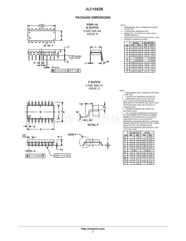
PDIP鈥?6
EIAJ鈥?6
EIAJ鈥?6
Shipping
500 / Unit Pak
50 Units / Rail
2000 Units / Reel
NOTE: Internal Power On Reset sets P0
鈭?/div>
P7 low, sets VDAC to 1/80 VDD
and selects 1/2 VDD for Comparator 鈥淏鈥?threshold.
Figure 1. Block Diagram
漏
Semiconductor Components Industries, LLC, 1999
1
March, 2000 鈥?Rev. 1
Publication Order Number:
JLC1562BE/D


 1
1
 2
2
 3
3
 4
4
 5
5
 6
6
 7
7
 8
8
