鈩?/div>
Clamped inductive load
T
C
= 25擄C
Maximum Ratings
1200
1200
鹵20
鹵30
30
15
60
I
CM
= 40
@ 0.8 V
CES
150
-55 ... +150
150
-55 ... +150
300
260
V
V
V
V
A
A
A
A
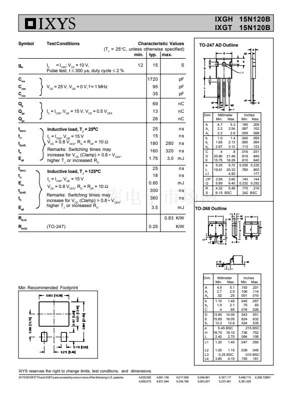
TO-268 (IXGT)
G
E
C (TAB)
TO-247 AD (IXGH)
G
C (TAB)
C
E
W
擄C
擄C
擄C
擄C
擄C
Features
G = Gate,
E = Emitter,
C = Collector,
TAB = Collector
Maximum Lead temperature for soldering
1.6 mm (0.062 in.) from case for 10 s
Maximum Tab temperature for soldering SMD devices for 10 s
M
d
Weight
Mounting torque (M3)
1.13/10Nm/lb.in.
TO-247 AD
TO-268
6
4
g
g
International standard packages
JEDEC TO-268 surface and
JEDEC TO-247 AD
Low switching losses, low V
(sat)
MOS Gate turn-on
- drive simplicity
Applications
Symbol
Test Conditions
Characteristic Values
(T
J
= 25擄C, unless otherwise specified)
min. typ. max.
1200
2.5
T
J
= 25擄C
T
J
= 125擄C
5
100
3.5
鹵100
3.2
T
J
= 125擄C
2.5
V
V
碌A(chǔ)
mA
nA
V
V
BV
CES
V
GE(th)
I
CES
I
GES
V
CE(sat)
I
C
I
C
= 250
碌A(chǔ),
V
GE
= 0 V
= 250
碌A(chǔ),
V
CE
= V
GE
AC motor speed control
DC servo and robot drives
DC choppers
Uninterruptible power supplies (UPS)
Switched-mode and resonant-mode
power supplies
Advantages
High power density
Suitable for surface mounting
Easy to mount with 1 screw,
(isolated mounting screw hole)
V
CE
= V
CES
V
GE
= 0 V
V
CE
= 0 V, V
GE
=
鹵20
V
I
C
= I
C90
, V
GE
= 15 V
漏 2002 IXYS All rights reserved
98659-A (7-02)


 1
1
 2
2
 3
3
 4
4
