ITF87008DQT
Data Sheet
March 2000
File Number
4814.2
7.0A, 20V, 0.023 Ohm, Dual N-Channel,
2.5V Speci鏗乪d Power MOSFET
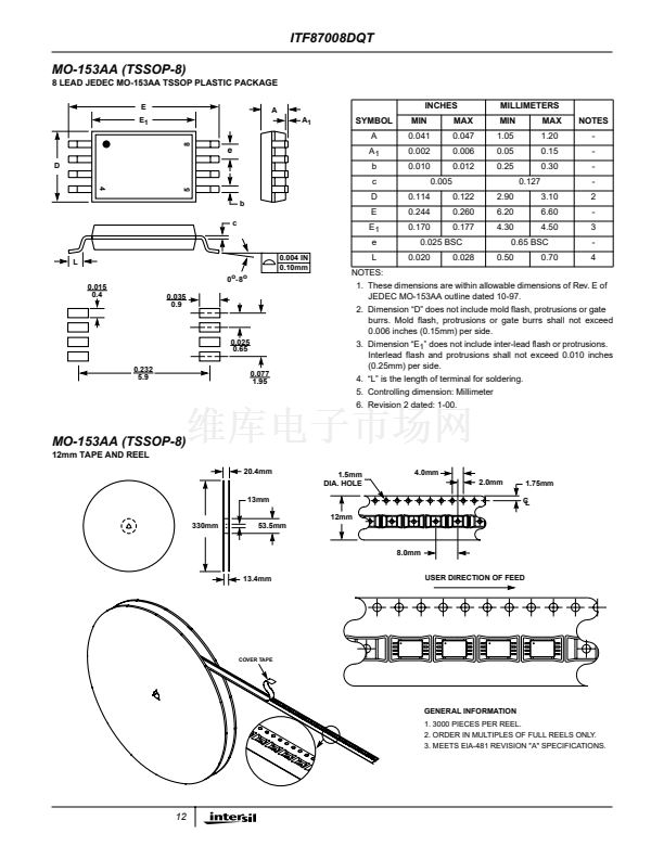
Packaging
TSSOP-8
Features
鈥?Ultra Low On-Resistance
- r
DS(ON)
= 0.023鈩?
V
GS
=
4.5V
- r
DS(ON)
= 0.024鈩?
V
GS
=
4.0V
- r
DS(ON)
= 0.029鈩?
V
GS
=
2.5V
鈥?2.5 Volt Gate Drive Capability
鈥?Gate to Source Protection Diode
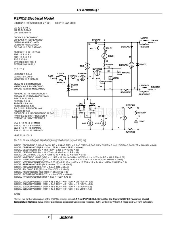
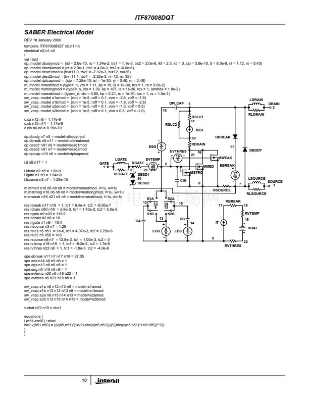
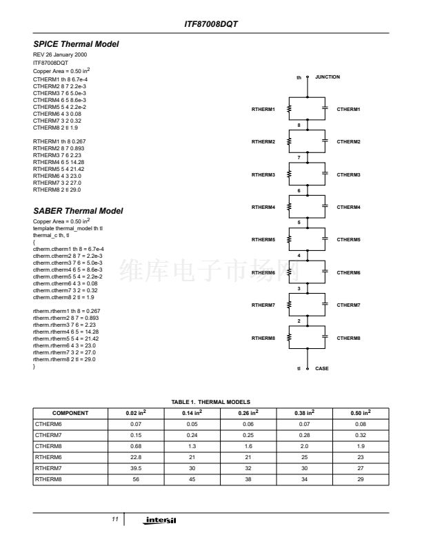
鈥?Simulation Models
- Temperature Compensated PSPICE鈩?and SABER
Electrical Models
- Spice and SABER Thermal Impedance Models
- www.intersil.com
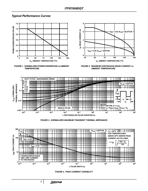
鈥?Peak Current vs Pulse Width Curve
鈥?Transient Thermal Impedance Curve vs Board Mounting
Area
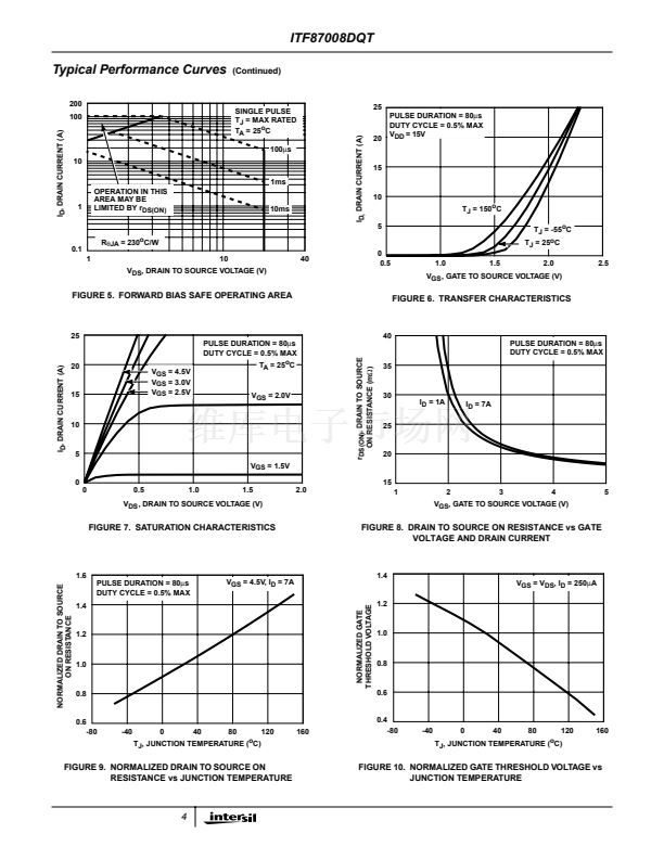
鈥?Switching Time vs R
GS
Curves
5
1
23
4
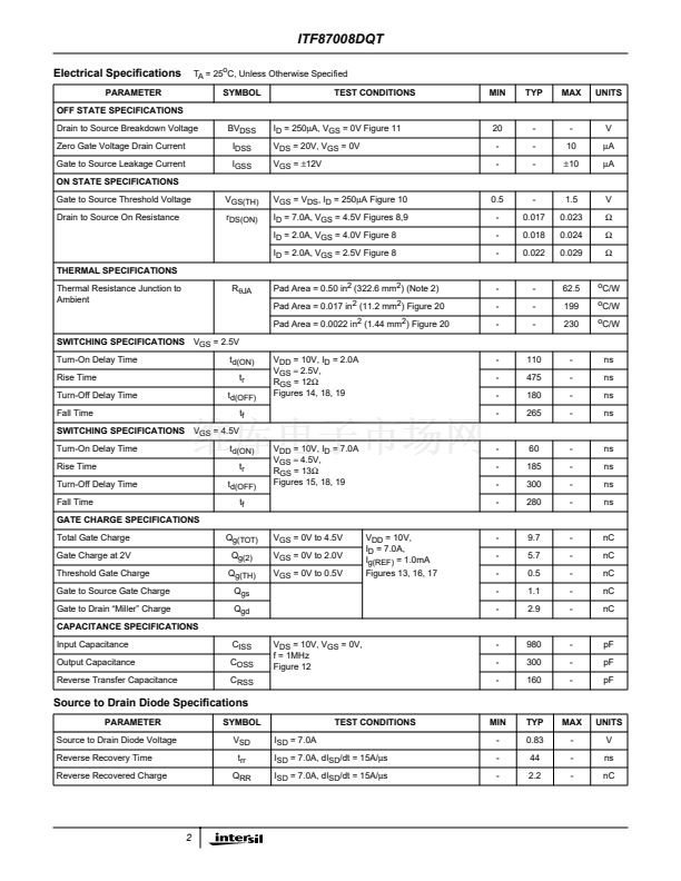
Symbol
DRAIN1(1)
SOURCE1(2)
SOURCE1(3)
GATE1(4)
(8) DRAIN2
(7) SOURCE2
(6) SOURCE2
(5) GATE2
Ordering Information
PART NUMBER
ITF87008DQT
PACKAGE
TSSOP-8
87008
BRAND
NOTE: When ordering, use the entire part number. ITF87008DQT2
is available only in tape and reel.
Absolute Maximum Ratings
T
A
= 25
o
C, Unless Otherwise Specified
ITF87008DQT
UNITS
V
V
V
A
A
A
A
W
mW/
o
C
o
C
o
C
o
C
Drain to Source Voltage (Note 1) . . . . . . . . . . . . . . . . . . . . . . . . . . . . . . . . . . . . . . . . . . V
DSS
Drain to Gate Voltage (R
GS
= 20k鈩? (Note 1) . . . . . . . . . . . . . . . . . . . . . . . . . . . . . . . . V
DGR
Gate to Source Voltage . . . . . . . . . . . . . . . . . . . . . . . . . . . . . . . . . . . . . . . . . . . . . . . . . . V
GS
Drain Current
Continuous (T
A
= 25
o
C, V
GS
= 4.5V) (Note 2) . . . . . . . . . . . . . . . . . . . . . . . . . . . . . . . . . I
D
Continuous (T
A
= 25
o
C, V
GS
= 4.0V) (Note 2) . . . . . . . . . . . . . . . . . . . . . . . . . . . . . . . . . I
D
Continuous (T
A
= 100
o
C, V
GS
= 4.0V) (Note 3) . . . . . . . . . . . . . . . . . . . . . . . . . . . . . . . . I
D
Continuous (T
A
= 100
o
C, V
GS
= 2.5V) (Note 3) . . . . . . . . . . . . . . . . . . . . . . . . . . . . . . . . I
D
Pulsed Drain Current . . . . . . . . . . . . . . . . . . . . . . . . . . . . . . . . . . . . . . . . . . . . . . . . . . .I
DM
Power Dissipation (Note 2) . . . . . . . . . . . . . . . . . . . . . . . . . . . . . . . . . . . . . . . . . . . . . . . . P
D
Derate Above 25
o
C . . . . . . . . . . . . . . . . . . . . . . . . . . . . . . . . . . . . . . . . . . . . . . . . . . . . . . .
Operating and Storage Temperature . . . . . . . . . . . . . . . . . . . . . . . . . . . . . . . . . . . . T
J
, T
STG
Maximum Temperature for Soldering
Leads at 0.063in (1.6mm) from Case for 10s. . . . . . . . . . . . . . . . . . . . . . . . . . . . . . . . . .T
L
Package Body for 10s, See Techbrief TB370 . . . . . . . . . . . . . . . . . . . . . . . . . . . . . . . . T
pkg
NOTES:
1. T
J
= 25
o
C to 125
o
C.
2. 62.5
o
C/W measured using FR-4 board with 0.50 in
2
(322.6 mm
2
) copper pad at 1 second.
3. 230
o
C/W measured using FR-4 board with 0.0022 in
2
(1.44 mm
2
) copper pad at 1000 seconds.
20
20
鹵12
7.0
7.0
2.0
2.0
Figure 4
2.0
16
-55 to 150
300
260
CAUTION:
Stresses above those listed in 鈥淎bsolute Maximum Ratings鈥?may cause permanent damage to the device. This is a stress only rating and operation of the
device at these or any other conditions above those indicated in the operational sections of this speci鏗乧ation is not implied.
1
CAUTION: These devices are sensitive to electrostatic discharge. Follow proper ESD Handling Procedures.
SABER漏 is a Copyright of Analogy Inc. PSPICE廬 is a registered trademark of MicroSim Corporation.
1-888-INTERSIL or 321-724-7143
|
Copyright
漏
Intersil Corporation 2000


 1
1
 2
2
 3
3
 4
4
 5
5
 6
6
 7
7
 8
8
 9
9
 10
10
 11
11
 12
12
 13
13
