ITF86110DK8T
Data Sheet
January 2000
File Number
4807.2
7.5A, 30V, 0.025 Ohm, Dual N-Channel,
Logic Level, Power MOSFET
Features
鈥?Ultra Low On-Resistance
- r
DS(ON)
= 0.025鈩?
V
GS
=
10V
- r
DS(ON)
= 0.034鈩?
V
GS
=
4.5V
- r
DS(ON)
= 0.042鈩?
V
GS
=
4.0V
鈥?Gate to Source Protection Diode
鈥?Simulation Models
- Temperature Compensated PSPICE鈩?and SABER
Electrical Models
- Spice and SABER Thermal Impedance Models
- www.intersil.com
[ /Title
Packaging
SO8 (JEDEC MS-012AA)
(HUF7
6400S
BRANDING DASH
K8)
/Sub-
5
ject
(60V,
1
0.072
2
3
4
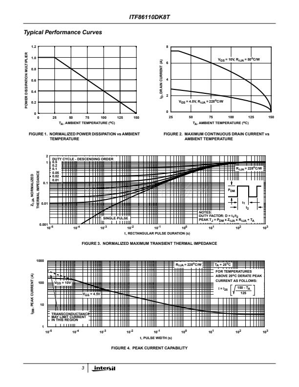
鈥?Peak Current vs Pulse Width Curve
Ohm,
4A, N-
鈥?Transient Thermal Impedance Curve vs Board Mounting
Area
Chan-
Symbol
nel,
鈥?Switching Time vs R
GS
Curves
DRAIN1(8)
DRAIN1(7)
Logic
SOURCE1(1)
Ordering Information
Level
GATE1(2)
UltraFE
PART NUMBER
PACKAGE
BRAND
DRAIN2(6)
T
ITF86110DK8T
SO8
86110
DRAIN2(5)
Power
NOTE: When ordering, use the entire part number. ITF86110DK8T
SOURCE2(3)
MOS-
is available only in tape and reel.
GATE2(4)
FET)
/Author
()
/Key-
Absolute Maximum Ratings
T
A
= 25
o
C, Unless Otherwise Specified
words
ITF86110DK8T
UNITS
(Inter-
Drain to Source Voltage (Note 1) . . . . . . . . . . . . . . . . . . . . . . . . . . . . . . . . . . . . . . . . . . V
DSS
30
V
sil
Drain to Gate Voltage (R
GS
= 20k鈩? (Note 1) . . . . . . . . . . . . . . . . . . . . . . . . . . . . . . . . V
DGR
30
V
Semi-
Gate to Source Voltage . . . . . . . . . . . . . . . . . . . . . . . . . . . . . . . . . . . . . . . . . . . . . . . . . . V
GS
鹵20
V
conduc-
Drain Current
Continuous (T
A
= 25
o
C, V
GS
= 10V) (Figure 2) (Note 2) . . . . . . . . . . . . . . . . . . . . . . . . . I
D
7.5
A
tor, N-
Continuous (T
A
= 25
o
C, V
GS
= 4.5V) (Note 2) . . . . . . . . . . . . . . . . . . . . . . . . . . . . . . . . . I
D
6.5
A
Chan-
o
C, V
Continuous (T
A
= 100
2.0
A
GS
= 4.5V) (Note 3) . . . . . . . . . . . . . . . . . . . . . . . . . . . . . . . . I
D
nel,
Continuous (T
A
= 100
o
C, V
GS
= 4.0V) (Note 3) . . . . . . . . . . . . . . . . . . . . . . . . . . . . . . . . I
D
1.5
A
Pulsed Drain Current . . . . . . . . . . . . . . . . . . . . . . . . . . . . . . . . . . . . . . . . . . . . . . . . . . .I
DM
Figure 4
A
Logic
Power Dissipation (Note 2) . . . . . . . . . . . . . . . . . . . . . . . . . . . . . . . . . . . . . . . . . . . . . . . . P
D
2.5
W
Level
Derate Above 25
o
C . . . . . . . . . . . . . . . . . . . . . . . . . . . . . . . . . . . . . . . . . . . . . . . . . . . . . . .
20
mW/
o
C
o
C
UltraFE
Operating and Storage Temperature . . . . . . . . . . . . . . . . . . . . . . . . . . . . . . . . . . . . T
J
, T
STG
-55 to 150
T
Maximum Temperature for Soldering
o
C
Leads at 0.063in (1.6mm) from Case for 10s. . . . . . . . . . . . . . . . . . . . . . . . . . . . . . . . . .T
L
300
Power
o
Package Body for 10s, See Tech brief TB370 . . . . . . . . . . . . . . . . . . . . . . . . . . . . . . . T
pkg
260
C
CAUTION:
Stresses above those listed in 鈥淎bsolute Maximum Ratings鈥?may cause permanent damage to the device. This is a stress only rating and operation of the
device at these or any other conditions above those indicated in the operational sections of this speci鏗乧ation is not implied.
NOTES:
1. T
J
= 25
o
C to 125
o
C.
2. 50
o
C/W measured using FR-4 board with 0.14 in
2
(90.3 mm
2
) copper pad at 1 second.
3. 228
o
C/W measured using FR-4 board with 0.006 in
2
(3.9 mm
2
) copper pad at 1000 second.
CAUTION: These devices are sensitive to electrostatic discharge. Follow proper ESD Handling Procedures.
PSPICE廬 is a registered trademark of MicroSim Corporation.
SABER漏 is a Copyright of Analogy Inc.http://www.intersil.com or 321-727-9207
|
1-888-INTERSIL or 321-724-7143
|
Copyright
漏
Intersil Corporation 2000
1


 1
1
 2
2
 3
3
 4
4
 5
5
 6
6
 7
7
 8
8
 9
9
 10
10
 11
11
 12
12
 13
13
