-
-

- 手機版
-

- 芯視頻 APP
-

- 微信公眾號
-

- 維庫官方抖音
-

- 微信頭條號
-
- |
- |
- |
- |

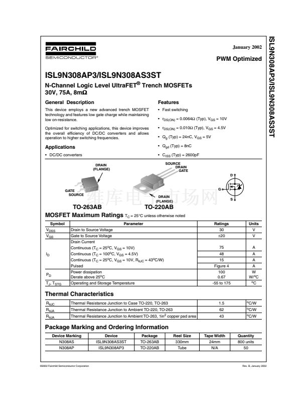
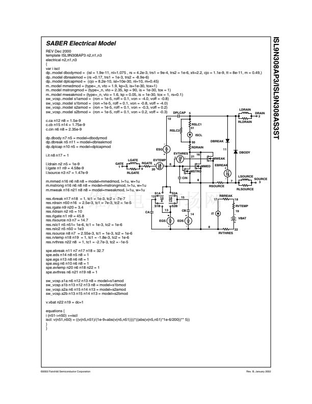
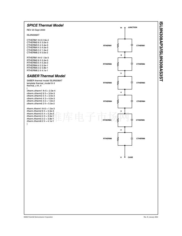
ISL9N308AS3ST
N-Channel Logic Level UltraFET Trench MOSFETs 30V, 75A, 8m ...
11頁
FAIRCHILD
掃碼查看芯片數(shù)據(jù)手冊
上傳產(chǎn)品規(guī)格書
Fairchild Semiconductor
MOSFET
N-Channel
30 V
+/- 20 V
75 A
0.008 Ohms
Single
+ 175 C
SMD/SMT
TO-263AB
Reel
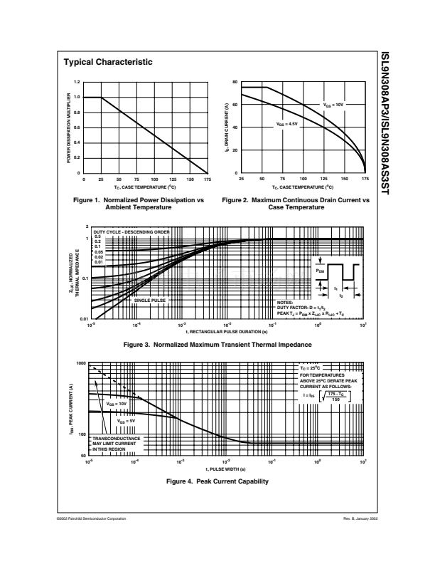
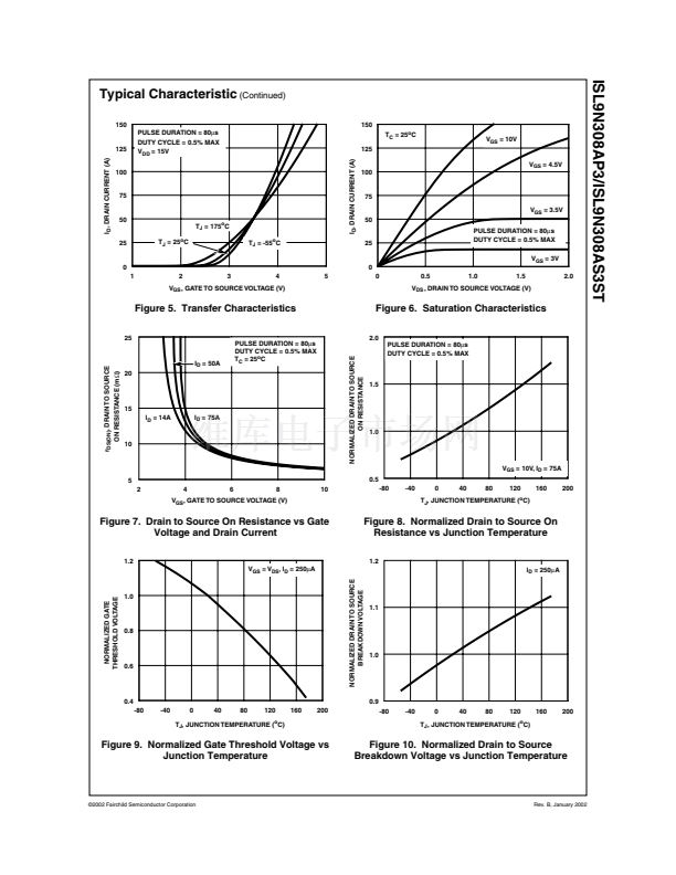
32 ns, 31 ns
- 55 C
100 W
67 ns, 40 ns
800
35 ns, 64 ns


聯(lián)系人:
聯(lián)系方式:

 1
1
 2
2
 3
3
 4
4
 5
5
 6
6
 7
7
 8
8
 9
9
 10
10
 11
11
