6.8m鈩?/div>
I
D
110A
聞
Ultra-Low Gate Impedance
Very Low RDS(on) at 4.5V V
GS
Fully Characterized Avalanche Voltage
and Current
D-Pak
IRLR8203
I-Pak
IRLU8203
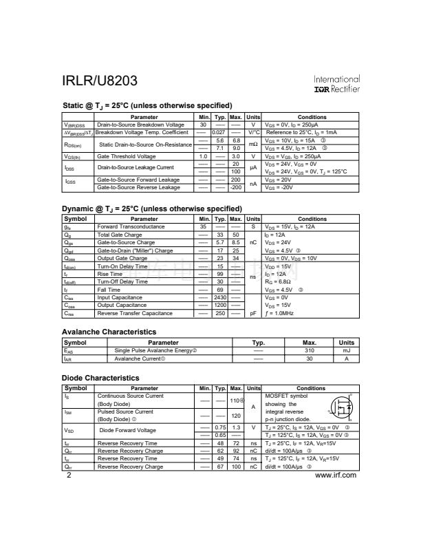
Absolute Maximum Ratings
Symbol
V
DS
V
GS
I
D
@ T
C
= 25擄C
I
D
@ T
C
= 100擄C
I
DM
P
D
@T
C
= 25擄C
P
D
@T
C
= 100擄C
T
J
, T
STG
Parameter
Drain-Source Voltage
Gate-to-Source Voltage
Continuous Drain Current, V
GS
@ 10V
Continuous Drain Current, V
GS
@ 10V
Pulsed Drain Current
聛
Maximum Power Dissipation
聝
Maximum Power Dissipation
聝
Linear Derating Factor
Junction and Storage Temperature Range
Max.
30
鹵 20
110
聞
76
聞
120
140
69
0.92
-55 to + 175
Units
V
V
A
W
W
W/擄C
擄C
Thermal Resistance
Parameter
R
胃JC
R
胃JA
R
胃JA
Junction-to-Case
Junction-to-Ambient (PCB mount)*
Junction-to-Ambient
Typ.
鈥撯€撯€?/div>
鈥撯€撯€?/div>
鈥撯€撯€?/div>
Max.
1.09
50
110
Units
擄C/W
* When mounted on 1" square PCB (FR-4 or G-10 Material) .
For recommended footprint and soldering techniques refer to application note #AN-994
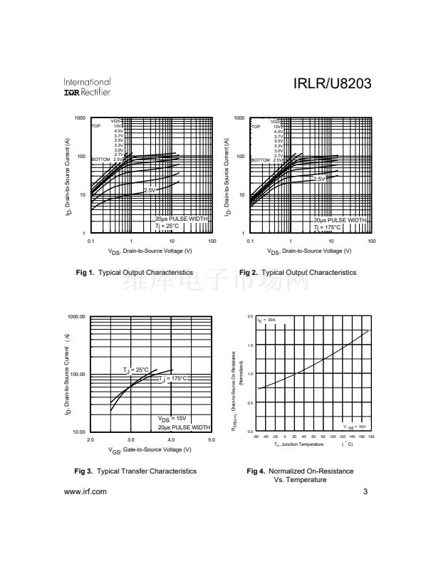
Notes
聛
through
聞
are on page 10
www.irf.com
1
03/12/02


 1
1
 2
2
 3
3
 4
4
 5
5
 6
6
 7
7
 8
8
 9
9
 10
10
