鈥?/div>
100% R
G
Tested
Description
This new device employs advanced HEXFET Power
MOSFET technology to achieve an unprecedented
balance of on-resistance and gate charge. The reduced
conduction and switching losses make it ideal for high
efficiency DC-DC converters that power the latest
generation of microprocessors.
The IRLR8103V has been optimized for all parameters
that are critical in synchronous buck converters including
R
DS(on)
, gate charge and Cdv/dt-induced turn-on immunity.
The IRLR8103V offers an extremely low combination of
Q
sw
& R
DS(on)
for reduced losses in both control and
synchronous FET applications.
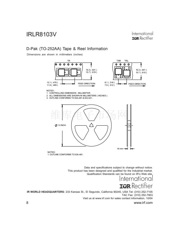
The package is designed for vapor phase, infra-red,
convection, or wave soldering techniques. Power
dissipation of greater than 2W is possible in a typical
PCB mount application.
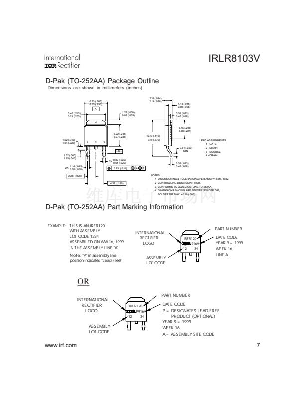
D-Pak
S
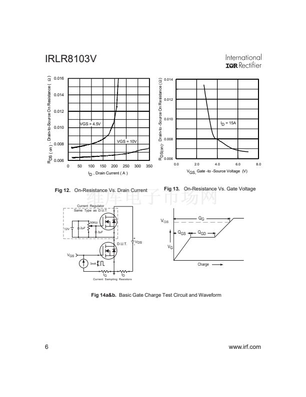
DEVICE CHARACTERISTICS聟
R
DS(on)
Q
G
Q
SW
Q
OSS
IRLR8103V
7.9 m鈩?/div>
27 nC
12 nC
29nC
Absolute Maximum Ratings
Parameter
Drain-Source Voltage
Gate-Source Voltage
Continuous Drain or Source Current
(V
GS
> 10V)
Pulsed Drain Current
TC = 25擄C
TC= 90擄C
Symbol
V
DS
V
GS
I
D
I
DM
P
D
T
J
, T
STG
I
S
I
SM
IRLR8103V
30
鹵20
91
63
363
115
60
-55 to 150
91
363
Units
V
聶
TC = 25擄C
Power Dissipation
e脙脙脙脙脙脙脙脙脙脙脙脙脙
TC = 90擄C
Junction & Storage Temperature Range
Continuous Source Current (Body Diode)
Pulsed Source Current
A
W
擄C
A
聶
Thermal Resistance
Parameter
Maximum Junction-to-Ambient
Maximum Junction-to-Case
h
eh
Symbol
R
胃JA
R
胃JC
Typ.
鈥撯€撯€?/div>
鈥撯€撯€?/div>
Max.
50
1.09
Units
擄C/W
www.irf.com
1
10/22/04


 1
1
 2
2
 3
3
 4
4
 5
5
 6
6
 7
7
 8
8
