low on-resistance per silicon area. This benefit, combined
餂?/div>
power MOSFETs are well known for, provides
the designer with an extremely efficient and reliable device
for use in battery and load management.
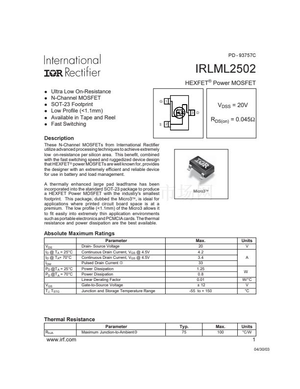
A thermally enhanced large pad leadframe has been
incorporated into the standard SOT-23 package to produce
a HEXFET Power MOSFET with the industry's smallest
footprint. This package, dubbed the Micro3錚? is ideal for
applications where printed circuit board space is at a
premium. The low profile (<1.1mm) of the Micro3 allows it
to fit easily into extremely thin application environments
such as portable electronics and PCMCIA cards. The thermal
resistance and power dissipation are the best available.
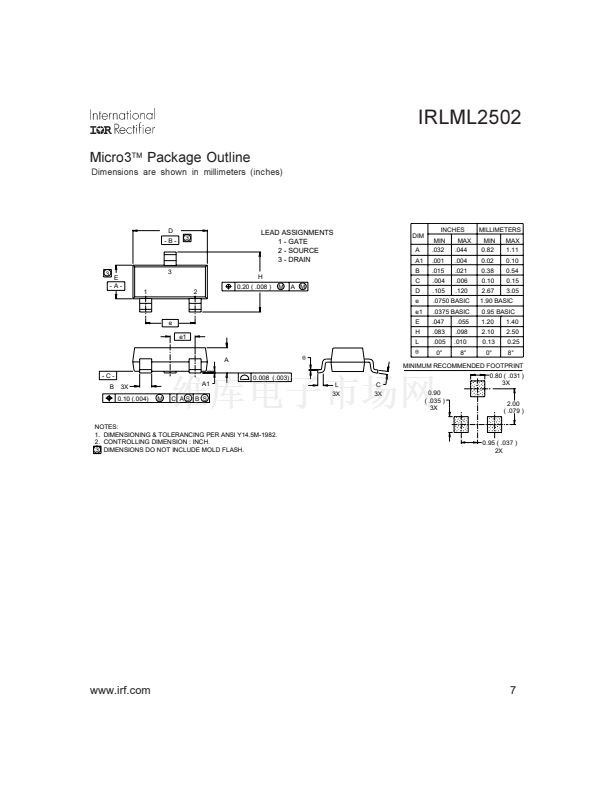
Micro3錚?/div>
Absolute Maximum Ratings
Parameter
V
DS
I
D
@ T
A
= 25擄C
I
D
@ T
A
= 70擄C
I
DM
P
D
@T
A
= 25擄C
P
D
@T
A
= 70擄C
V
GS
T
J,
T
STG
Drain- Source Voltage
Continuous Drain Current, V
GS
@ 4.5V
Continuous Drain Current, V
GS
@ 4.5V
Pulsed Drain Current
聛
Power Dissipation
Power Dissipation
Linear Derating Factor
Gate-to-Source Voltage
Junction and Storage Temperature Range
Max.
20
4.2
3.4
33
1.25
0.8
0.01
鹵 12
-55 to + 150
Units
V
A
W
W/擄C
V
擄C
Thermal Resistance
Parameter
R
胃JA
Maximum Junction-to-Ambient聝
Typ.
75
Max.
100
Units
擄C/W
www.irf.com
1
04/30/03


 1
1
 2
2
 3
3
 4
4
 5
5
 6
6
 7
7
 8
8
 9
9
