PD - 93891A
Ignition IGBT
Features
聲
Most Rugged in Industry
聲
Logic-Level Gate Drive
聲
> 6KV ESD Gate Protection
聲
Low Saturation Voltage
聲
High Self-clamped Inductive Switching Energy
The advanced IGBT process family includes a
MOS gated, N-channel logic level device which
is intended for coil-on-plug automotive ignition
applications and small-engine ignition circuits.
Unique features include on-chip active voltage
clamps between the Gate-Emitter and
Gate-Collector which provide over voltage
protection capability in ignition circuits.
Absolute Maximum Ratings
Parameter
Max
Clamped
20
14
1
10
Clamped
125
54
- 40 to 175
- 40 to 175
6
11.5
Unit
V
A
A
mA
IGBT with on-chip Gate-Emitter and Gate-Collector clamps
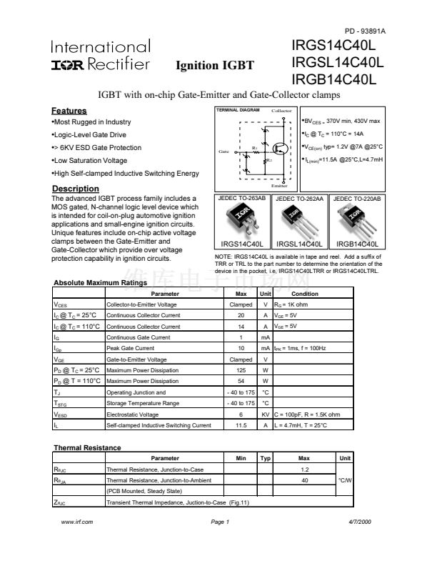
TERMINAL DIAGRAM
Collector
IRGS14C40L
IRGSL14C40L
IRGB14C40L
聲
BV
CES =
370V min, 430V max
聲
I
C
@ T
C
= 110擄C = 14A
聲
V
CE(on)
typ= 1.2V @7A @25擄C
聲
I
L(min)
=11.5A @25擄C,L=4.7mH
Gate
R
1
R
2
Description
Emitter
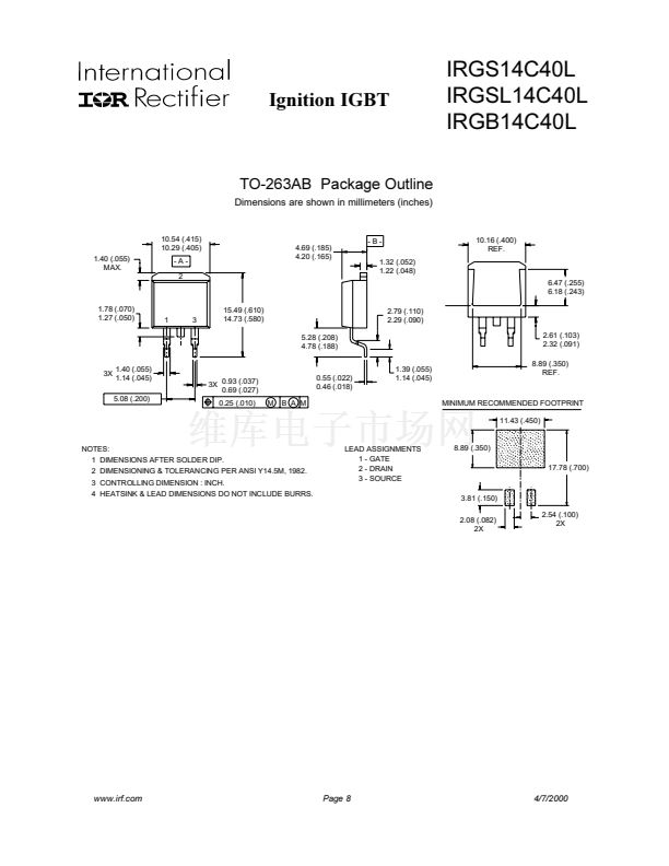
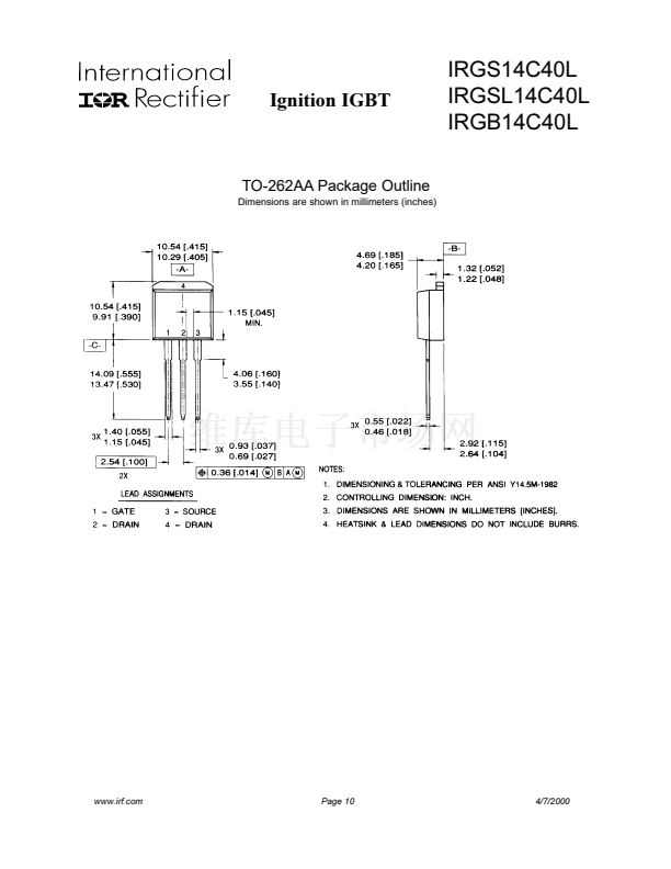
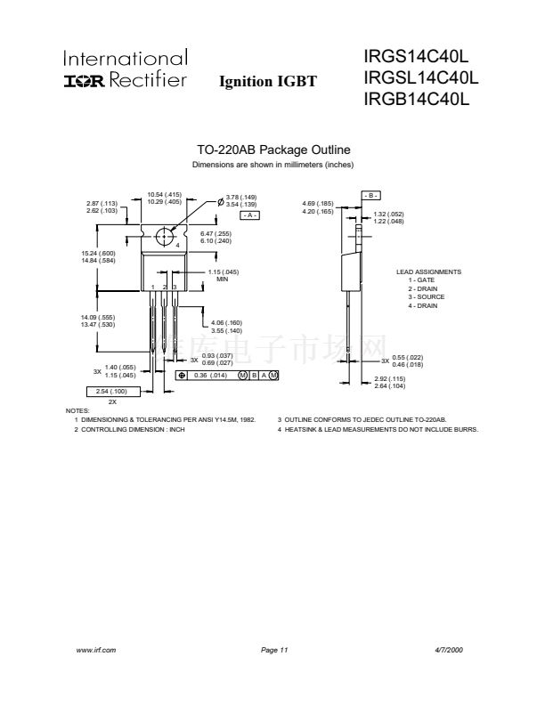
JEDEC TO-263AB
JEDEC TO-262AA
JEDEC TO-220AB
IRGS14C40L
IRGSL14C40L
IRGB14C40L
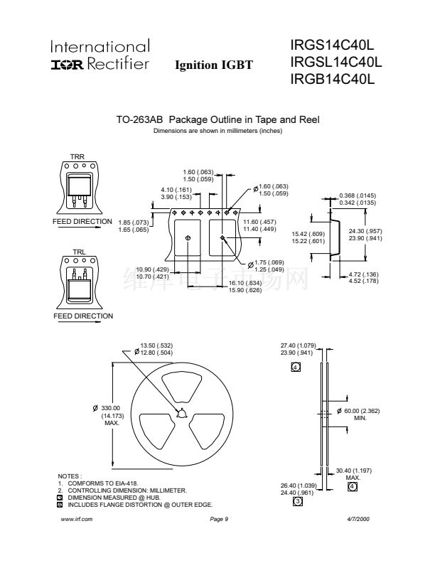
NOTE: IRGS14C40L is available in tape and reel. Add a suffix of
TRR or TRL to the part number to determine the orientation of the
device in the pocket, i.e, IRGS14C40LTRR or IRGS14C40LTRL.
Condition
R
G
= 1K
ohm
V
GE
= 5V
V
GE
= 5V
V
CES
I
C
@ T
C
= 25擄C
I
C
@ T
C
= 110擄C
I
G
I
Gp
V
GE
P
D
@ T
C
= 25擄C
T
J
T
STG
V
ESD
I
L
Collector-to-Emitter Voltage
Continuous Collector Current
Continuous Collector Current
Continuous Gate Current
Peak Gate Current
Gate-to-Emitter Voltage
Maximum Power Dissipation
mA t
PK
= 1ms, f = 100Hz
V
W
W
擄C
擄C
KV C = 100pF, R = 1.5K
ohm
A
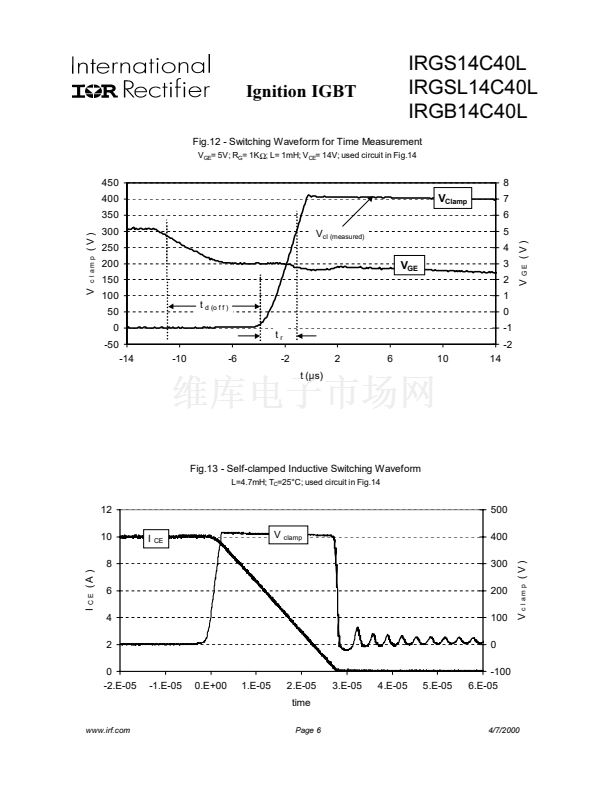
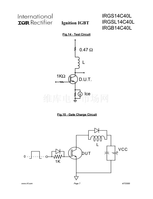
L = 4.7mH, T = 25擄C
P
D
@ T = 110擄C
Maximum Power Dissipation
Operating Junction and
Storage Temperature Range
Electrostatic Voltage
Self-clamped Inductive Switching Current
Thermal Resistance
Parameter
Min
Typ
Max
1.2
40
擄C/W
Unit
R
胃
JC
R
胃
JA
Z
胃
JC
www.irf.com
Thermal Resistance, Junction-to-Case
Thermal Resistance, Junction-to-Ambient
(PCB Mounted, Steady State)
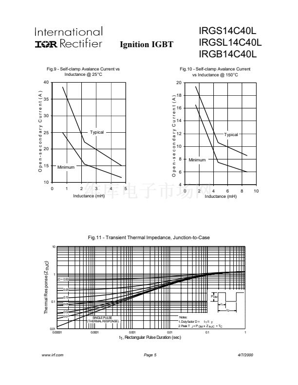
Transient Thermal Impedance, Juction-to-Case (Fig.11)
Page 1
4/7/2000


 1
1
 2
2
 3
3
 4
4
 5
5
 6
6
 7
7
 8
8
 9
9
 10
10
 11
11
