PD- 91758
IRG4CC30FB
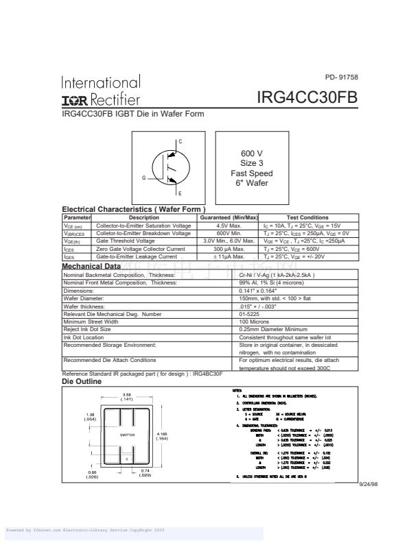
IRG4CC30FB IGBT Die in Wafer Form
C
G
E
600 V
Size 3
Fast Speed
6" Wafer
Electrical Characteristics ( Wafer Form )
Parameter
V
CE (on)
V
(BR)CES
V
GE(th)
I
CES
I
GES
Description
Collector-to-Emitter Saturation Voltage
Colletor-to-Emitter Breakdown Voltage
Gate Threshold Voltage
Zero Gate Voltage Collector Current
Gate-to-Emitter Leakage Current
Guaranteed (Min/Max)
4.5V Max.
600V Min.
3.0V Min., 6.0V Max.
300 碌A(chǔ) Max.
鹵
11碌A(chǔ) Max.
Test Conditions
I
C
= 10A, T
J
= 25擄C, V
GE
= 15V
T
J
= 25擄C, I
CES
= 250碌A(chǔ), V
GE
= 0V
V
GE
= V
CE
, T
J
=25擄C, I
C
=250碌A(chǔ)
T
J
= 25擄C, V
CE
= 600V
T
J
= 25擄C, V
GE
= +/- 20V
Mechanical Data
Nominal Backmetal Composition, Thickness:
Nominal Front Metal Composition, Thickness:
Dimensions:
Wafer Diameter:
Wafer thickness:
Relevant Die Mechanical Dwg. Number
Minimum Street Width
Reject Ink Dot Size
Ink Dot Location
Recommended Storage Environment:
Recommended Die Attach Conditions
Reference Standard IR packaged part ( for design ) : IRG4BC30F
Cr-Ni / V-Ag (1 kA-2kA-2.5kA )
99% Al, 1% Si (4 microns)
0.141" x 0.164"
150mm, with std. < 100 > flat
.015" + / -.003"
01-5225
100 Microns
0.25mm Diameter Minimum
Consistent throughout same wafer lot
Store in original container, in dessicated
nitrogen, with no contamination
For optimum electrical results, die attach
temperature should not exceed 300C
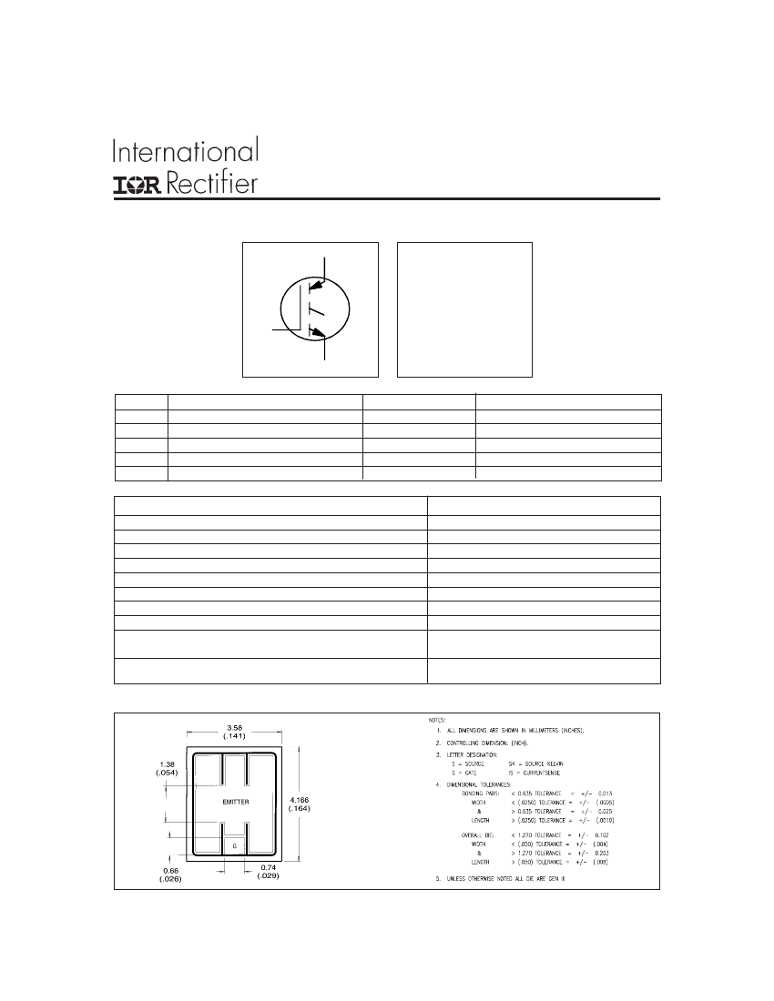
Die Outline
9/24/98
Powered by ICminer.com Electronic-Library Service CopyRight 2003


 1
1
