PD - 91790
IRG4BC30W-S
INSULATED GATE BIPOLAR TRANSISTOR
Features
鈥?Designed expressly for Switch-Mode Power
Supply and PFC (power factor correction)
applications
鈥?Industry-benchmark switching losses improve
efficiency of all power supply topologies
鈥?50% reduction of Eoff parameter
鈥?Low IGBT conduction losses
鈥?Latest-generation IGBT design and construction offers
tighter parameters distribution, exceptional reliability
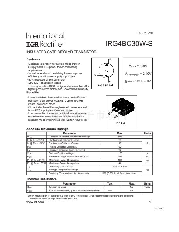
C
V
CES
= 600V
G
E
V
CE(on) typ.
= 2.10V
@V
GE
= 15V, I
C
= 12A
n-channel
Benefits
鈥?Lower switching losses allow more cost-effective
operation than power MOSFETs up to 150 kHz
("hard switched" mode)
鈥?Of particular benefit to single-ended converters and
boost PFC topologies 150W and higher
鈥?Low conduction losses and minimal minority-carrier
recombination make these an excellent option for
resonant mode switching as well (up to >>300 kHz)
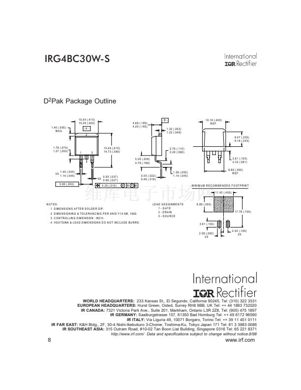
D
2
Pak
Absolute Maximum Ratings
Parameter
V
CES
I
C
@ T
C
= 25擄C
I
C
@ T
C
= 100擄C
I
CM
I
LM
V
GE
E
ARV
P
D
@ T
C
= 25擄C
P
D
@ T
C
= 100擄C
T
J
T
STG
Collector-to-Emitter Breakdown Voltage
Continuous Collector Current
Continuous Collector Current
Pulsed Collector Current
聛
Clamped Inductive Load Current
聜
Gate-to-Emitter Voltage
Reverse Voltage Avalanche Energy
聝
Maximum Power Dissipation
Maximum Power Dissipation
Operating Junction and
Storage Temperature Range
Soldering Temperature, for 10 seconds
Max.
600
23
12
92
92
鹵 20
180
100
42
-55 to + 150
300 (0.063 in. (1.6mm from case )
Units
V
A
V
mJ
W
擄C
Thermal Resistance
Parameter
R
胃JC
R
胃JA
Junction-to-Case
Junction-to-Ambient, ( PCB Mounted,steady-state)*
Typ.
鈥撯€撯€?/div>
鈥撯€撯€?/div>
Max.
1.2
40
Units
擄C/W
*
When mounted on 1" square PCB (FR-4 or G-10 Material ). For recommended footprint and soldering
techniques refer to application note #AN-994.
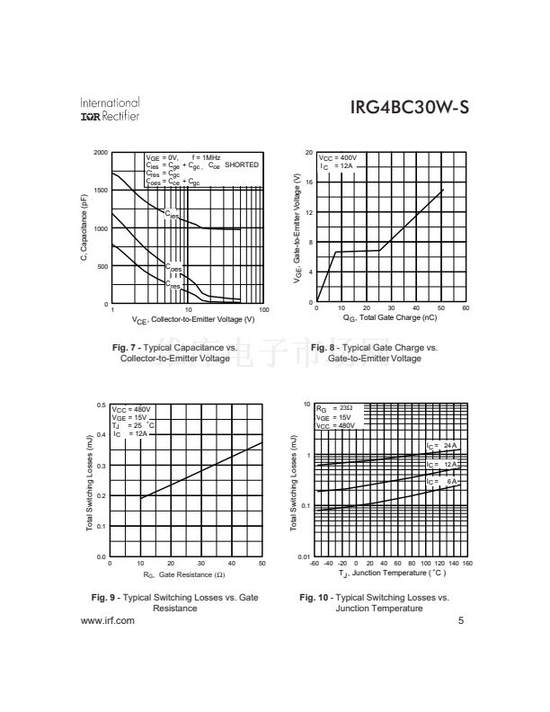
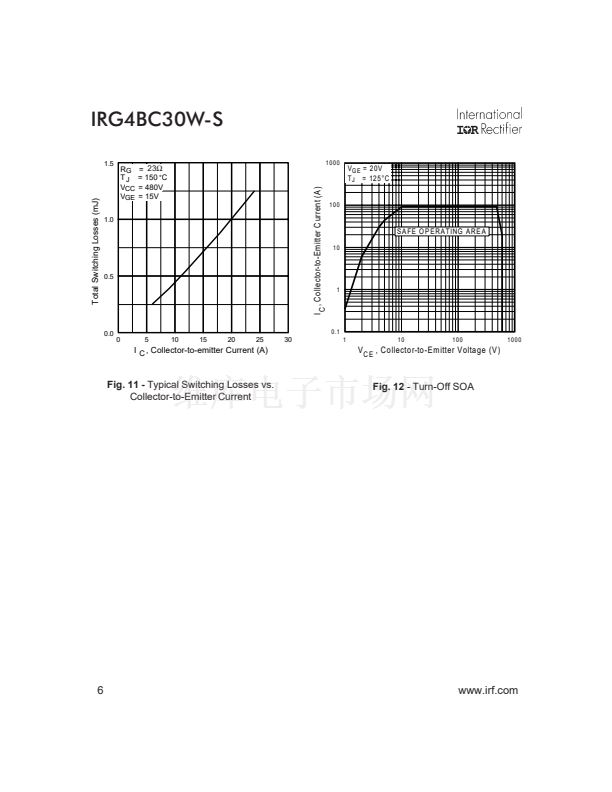
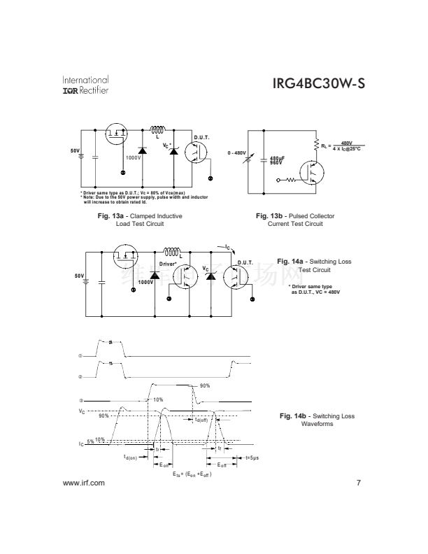
www.irf.com
1
8/13/98


 1
1
 2
2
 3
3
 4
4
 5
5
 6
6
 7
7
 8
8
