鈥?/div>
2.0A, 400V, R
DS(on)
= 3.4鈩?@V
GS
= 10 V
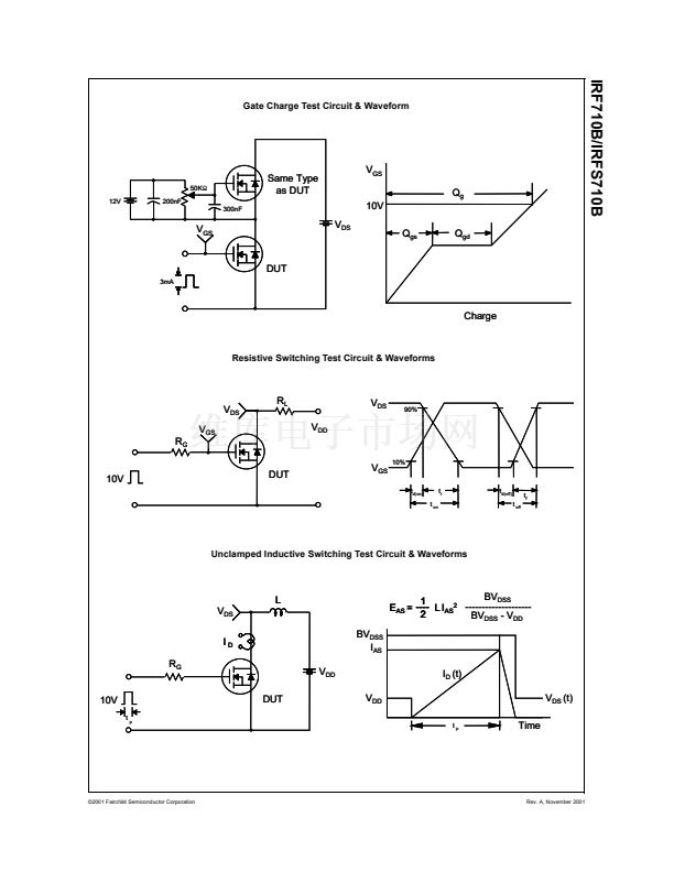
Low gate charge ( typical 7.7 nC)
Low Crss ( typical 6.0 pF)
Fast switching
100% avalanche tested
Improved dv/dt capability
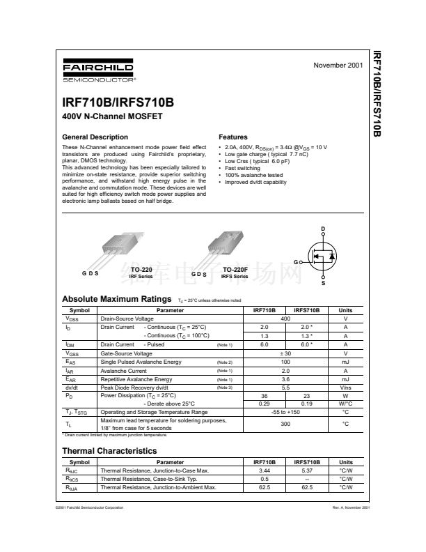
D
G
G DS
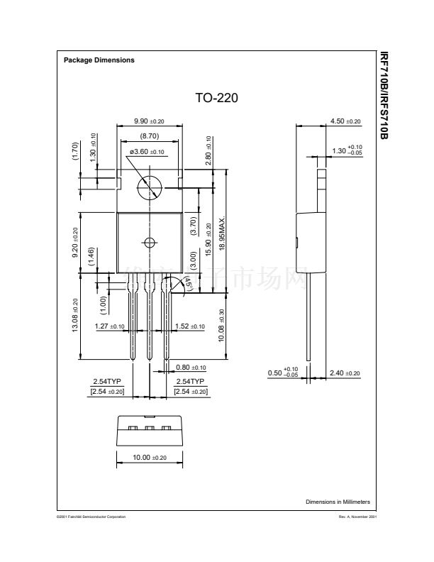
TO-220
IRF Series
GD S
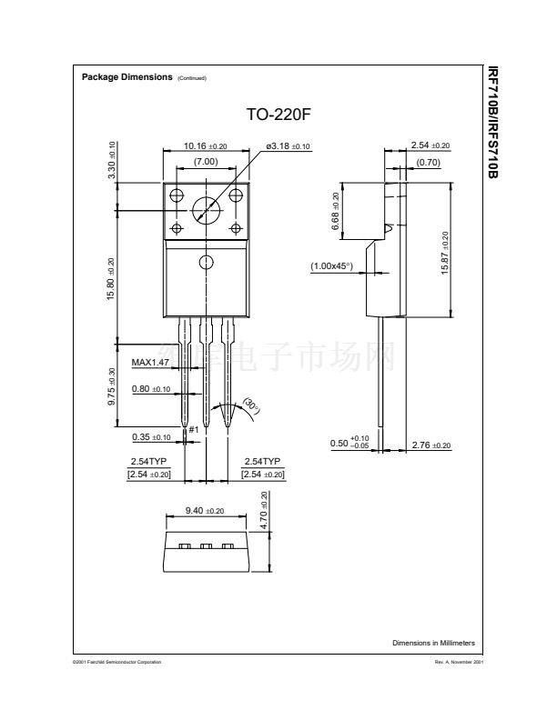
TO-220F
IRFS Series
S
Absolute Maximum Ratings
Symbol
V
DSS
I
D
I
DM
V
GSS
E
AS
I
AR
E
AR
dv/dt
P
D
T
J
, T
STG
T
L
T
C
= 25擄C unless otherwise noted
Parameter
Drain-Source Voltage
- Continuous (T
C
= 25擄C)
Drain Current
- Continuous (T
C
= 100擄C)
Drain Current
- Pulsed
(Note 1)
IRF710B
400
2.0
1.3
6.0
鹵
30
(Note 2)
(Note 1)
(Note 1)
(Note 3)
IRFS710B
2.0 *
1.3 *
6.0 *
100
2.0
3.6
5.5
Units
V
A
A
A
V
mJ
A
mJ
V/ns
W
W/擄C
擄C
擄C
Gate-Source Voltage
Single Pulsed Avalanche Energy
Avalanche Current
Repetitive Avalanche Energy
Peak Diode Recovery dv/dt
Power Dissipation (T
C
= 25擄C)
- Derate above 25擄C
Operating and Storage Temperature Range
Maximum lead temperature for soldering purposes,
1/8" from case for 5 seconds
36
0.29
-55 to +150
300
23
0.19
* Drain current limited by maximum junction temperature.
Thermal Characteristics
Symbol
R
胃JC
R
胃CS
R
胃JA
Parameter
Thermal Resistance, Junction-to-Case Max.
Thermal Resistance, Case-to-Sink Typ.
Thermal Resistance, Junction-to-Ambient Max.
IRF710B
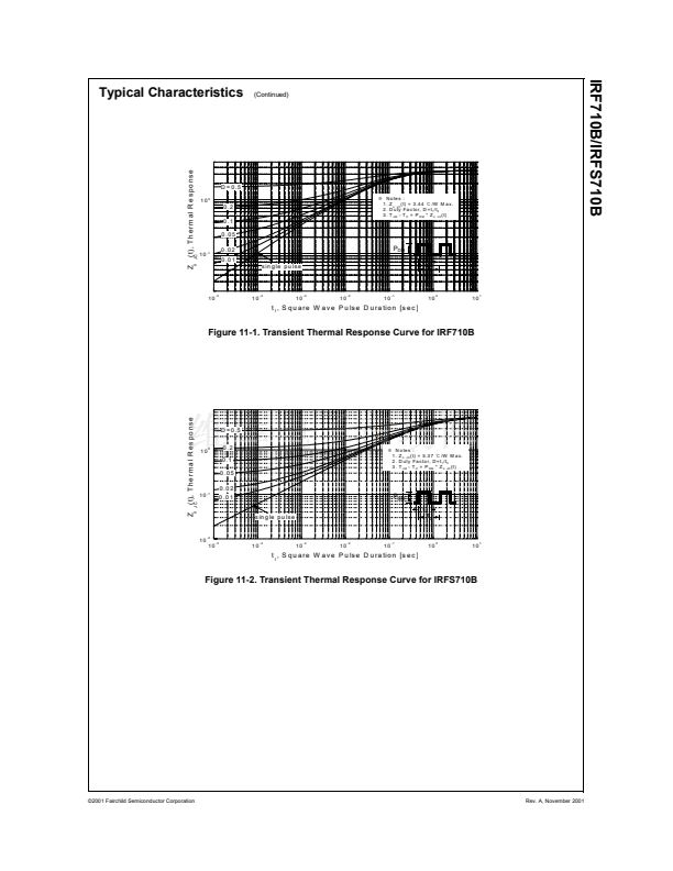
3.44
0.5
62.5
IRFS710B
5.37
--
62.5
Units
擄C/W
擄C/W
擄C/W
漏2001 Fairchild Semiconductor Corporation
Rev. A, November 2001


 1
1
 2
2
 3
3
 4
4
 5
5
 6
6
 7
7
 8
8
 9
9
 10
10
