IRFN340SMD
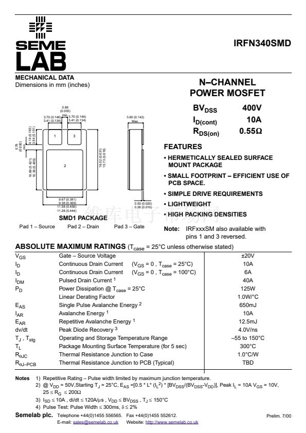
MECHANICAL DATA
Dimensions in mm (inches)
N鈥揅HANNEL
POWER MOSFET
3 .6 0 (0 .1 4 2 )
M a x .
0 .8 9
(0 .0 3 5 )
m in .
3 .7 0 (0 .1 4 6 )
3 .7 0 (0 .1 4 6 )
3 .4 1 (0 .1 3 4 )
3 .4 1 (0 .1 3 4 )
4 .1 4 (0 .1 6 3 )
3 .8 4 (0 .1 5 1 )
1
3
BV
DSS
I
D(cont)
R
DS(on)
FEATURES
400V
10A
0.55
W
0 .7 6
(0 .0 3 0 )
m in .
1 6 .0 2 (0 .6 3 1 )
1 5 .7 3 (0 .6 1 9 )
1 0 .6 9 (0 .4 2 1 )
1 0 .3 9 (0 .4 0 9 )
2
鈥?HERMETICALLY SEALED SURFACE
MOUNT PACKAGE
鈥?SMALL FOOTPRINT 鈥?EFFICIENT USE OF
PCB SPACE.
鈥?SIMPLE DRIVE REQUIREMENTS
9 .6
9 .3
1 1 .5
1 1 .2
7 (0
8 (0
8 (0
8 (0
.3 8
.3 6
.4 5
.4 4
1 )
9 )
6 )
4 )
0 .5 0 (0 .0 2 0 )
0 .2 6 (0 .0 1 0 )
鈥?LIGHTWEIGHT
鈥?HIGH PACKING DENSITIES
SMD1 PACKAGE
Pad 1 鈥?Source
Pad 2 鈥?Drain
Pad 3 鈥?Gate
Note:
IRFxxxSM also available with
pins 1 and 3 reversed.
鹵20V
10A
6A
40A
125W
1.0W/擄C
650mJ
10A
12.5mJ
4.0V/ns
鈥?5 to 150擄C
300擄C
1.0擄C/W
TBD
ABSOLUTE MAXIMUM RATINGS
(T
case
= 25擄C unless otherwise stated)
V
GS
I
D
I
D
I
DM
P
D
E
AS
I
AR
E
AR
dv/dt
T
J
, T
stg
T
L
R
q
JC
R
q
J鈥揚CB
Notes
1)
2)
2)
3)
4)
Gate 鈥?Source Voltage
Continuous Drain Current
(V
GS
= 0 , T
case
= 25擄C)
Continuous Drain Current
(V
GS
= 0 , T
case
= 100擄C)
Pulsed Drain Current
1
Power Dissipation @ T
case
= 25擄C
Linear Derating Factor
Single Pulse Avalanche Energy
2
Avalanche Energy
1
Repetitive Avalanche Energy
1
Peak Diode Recovery
3
Operating and Storage Temperature Range
Package Mounting Surface Temperature (for 5 sec)
Thermal Resistance Junction to Case
Thermal Resistance Junction to PCB (Typical)
Repetitive Rating 鈥?Pulse width limited by maximum junction temperature.
@ V
DD
= 50V,Starting T
J
= 25擄C, E
AS
=[0.5 * L* (I
L2
) * [BV
DSS
/(BV
DSS
-V
DD
)], Peak I
L
= 10A V
GS
= 10V,
25
攏
R
G
攏
200
W
I
SD
攏
10A , di/dt
攏
120A/
m
s , V
DD
攏
BV
DSS
, T
J
攏
150擄C
Pulse Test: Pulse Width
攏
300ms,
d 攏
2%
Telephone +44(0)1455 556565. Fax +44(0)1455 552612.
E-mail:
sales@semelab.co.uk
Website:
http://www.semelab.co.uk
Prelim. 7/00
Semelab plc.


 1
1
 2
2
