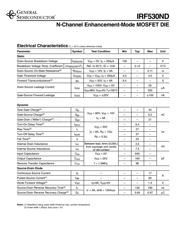
0.11鈩?/div>
I
D
17A
uct
rod
wP
Ne
G
D
Source
Physical Characteristics
鈥?Die size : 3890
X
1880
碌m
(153.1
X
74.0 mils)
鈥?Metalization:
Top:
Al/Si/Cu
Back: Ti/Ni/Ag
鈥?Metal Thickness:
Top:
3.0
碌m
Back: 1.4
碌m
鈥?Die thickness: 9 - 13 mils
鈥?Bonding Area:
Source: Full metalized surface of source region
Gate: 412 x 512
碌m
鈥?Recommended Wire Bonding:
Source: 12 mil diameter Al wire (2 wires preferred)
Gate: 5 mil diameter Al wire
Features
S
鈥?Dynamic dv/dt Rating 鈥?Repetitive Avalanche Rated
鈥?175擄C Operating Temperature 鈥?Ease of Paralleling
鈥?Fast Switching for High Efficiency
鈥?Simple Drive Requirements
鈥?Planar Technology
Maximum Ratings
Parameter
Drain-Source Voltage
Gate-Source Voltage
Continuous Drain Current
V
GS
=10V
Pulsed Drain Current
(1)
(T
A
= 25擄C unless otherwise noted)
Symbol
V
DS
V
GS
T
C
= 25擄C
T
C
= 100擄C
I
D
I
DM
T
C
= 25擄C
P
D
Limit
100
Unit
V
V
鹵
20
17
12
60
79
0.53
A
W
W/擄C
mJ
A
mJ
V/ns
擄C
Maximum Power Dissipation
Linear Derating Factor
Single Pulse Avalanche Energy
(2)
Avalanche Current
(1)
Repetitive Avalanche Energy
(1)
Peak Diode Recovery
(3)
E
AS
I
AR
E
AR
dv/dt
T
J
, T
stg
150
9
7.9
5.0
鈥?5 to 175
Operating Junction and Storage Temperature Range
Notes:
(1) Repetitive rating; pulse width limited by max. junction temperature
(2) V
DD
= 25V, starting T
J
= 25擄C, L = 3.1碌H, R
G
= 25鈩? I
AS
= 9.0A
(3) I
SD


 1
1
 2
2
 3
3
 4
4
 5
5
