IPD06N03LA
IPS06N03LA
IPF06N03LA
IPU06N03LA
OptiMOS
廬
2 Power-Transistor
Features
鈥?Ideal for high-frequency dc/dc converters
鈥?Qualified according to JEDEC for target application
鈥?N-channel, logic level
鈥?Excellent gate charge x
R
DS(on)
product (FOM)
鈥?Superior thermal resistance
鈥?175 擄C operating temperature
1)
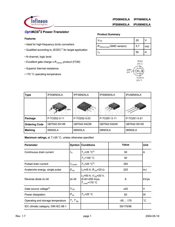
Product Summary
V
DS
R
DS(on),max
(SMD version)
I
D
25
5.7
50
V
m鈩?/div>
A
Type
IPD06N03LA
IPF06N03LA
IPS06N03LA
IPU06N03LA
Package
Ordering Code
Marking
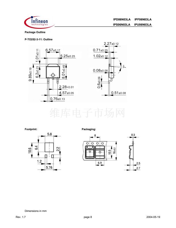
P-TO252-3-11
Q67042-S4149
06N03LA
P-TO252-3-23
Q67042-S4236
06N03LA
P-TO251-3-11
Q67042-S4245
06N03LA
P-TO251-3-21
Q67042-S4145
06N03LA
Maximum ratings,
at
T
j
=25 擄C, unless otherwise specified
Parameter
Continuous drain current
Symbol Conditions
I
D
T
C
=25 擄C
2)
T
C
=100 擄C
Pulsed drain current
Avalanche energy, single pulse
Reverse diode dv /dt
Gate source voltage
4)
Power dissipation
Operating and storage temperature
IEC climatic category; DIN IEC 68-1
I
D,pulse
E
AS
dv /dt
V
GS
P
tot
T
j
,
T
stg
T
C
=25 擄C
T
C
=25 擄C
3)
I
D
=45 A,
R
GS
=25
鈩?/div>
I
D
=50 A,
V
DS
=20 V,
di /dt =200 A/碌s,
T
j,max
=175 擄C
Value
50
50
350
225
6
鹵20
83
-55 ... 175
55/175/56
mJ
kV/碌s
V
W
擄C
Unit
A
Rev. 1.7
page 1
2004-05-19


 1
1
 2
2
 3
3
 4
4
 5
5
 6
6
 7
7
 8
8
 9
9
 10
10
 11
11
