;
IOP 480 AA
Design Note Rev. 1.3
March 2002
Design Note Documentation
A.
Affected Silicon Revision
Part Number
IOP480-AA60PI
IOP480-AA66PI
IOP480-AA60BI
IOP480-AA66BI
Description
60MHz Local Bus
208-pin PQFP Product
66MHz Local Bus
208-pin PQFP Product
60MHz Local Bus
225-pin PBGA Product
66MHz Local Bus
225-pin PBGA Product
Status
In production October 1999
In production October 1999
In production October 1999
In production October 1999
This document details Design Notes for the following silicon:
Product
IOP 480 AA
IOP 480 AA
IOP 480 AA
IOP 480 AA
B.
Documentation Status
The following documentation is the baseline functional description of the silicon.
Errata are defined as behaviors in the affected silicon that do not match
behaviors detailed in this documentation.
Document
IOP 480 Data Book
IOP 480 AA Errata
Revision
2.0
See
www.plxtech.com
for latest revision
Description
Released Data Book
IOP 480 Errata
Documentation
Publication Date
July 2000
C.
#
1
2
3
4
5
6
7
8
9
10
11
12
Design Note Summary
Description
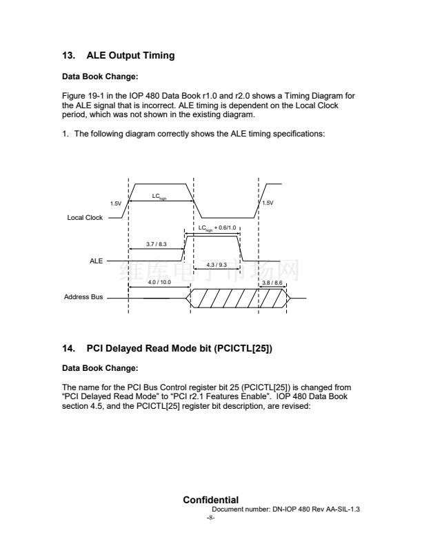
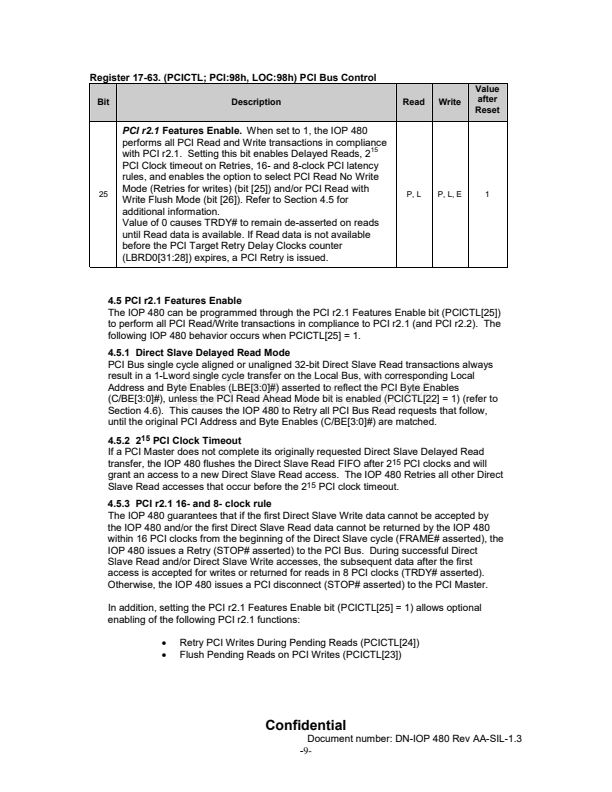
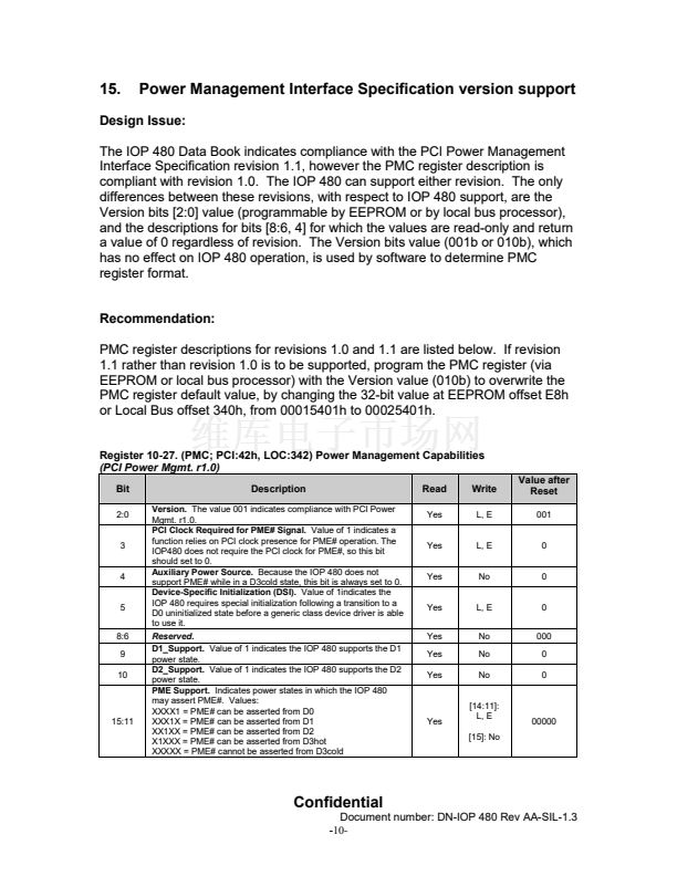
End-of-Transfer (EOT) During Chaining DMA End Link Mode with Write-back
DMA Channel 2 with End-of-Transfer (EOTx#) asserted coincident with ADS#
Zero Wait State SRAM Writes
External local master write to IOP 480 internal configuration registers with WAIT# being used
to insert wait states
Modifying internal configuration registers that affect on-going transfers
Operation of IOP 480 Buffers in 3.3 Volt Signaling Environment
LCSx# Chip Select output delayed when IOP 480 is initiating access to SRAM
CompactPCI Hot Swap Insertion Bit Status
DMPAF# (Direct Master Programmable Almost Full) negation timing
Messaging Unit data corruption if Queue Prefetch (Inbound Free List FIFO Prefetch and/or
Outbound Post List FIFO Prefetch) is enabled
Local Bus Timeout with SDRAM
WAIT# input signal when using the Memory Controller
Confidential
Document number: DN-IOP 480 Rev AA-SIL-1.3
-1-


 1
1
 2
2
 3
3
 4
4
 5
5
 6
6
 7
7
 8
8
 9
9
 10
10
 11
11
