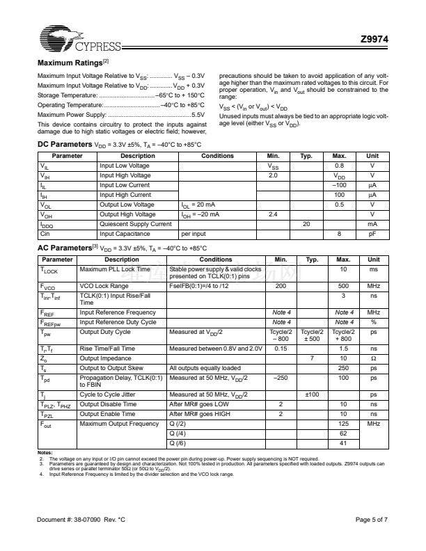
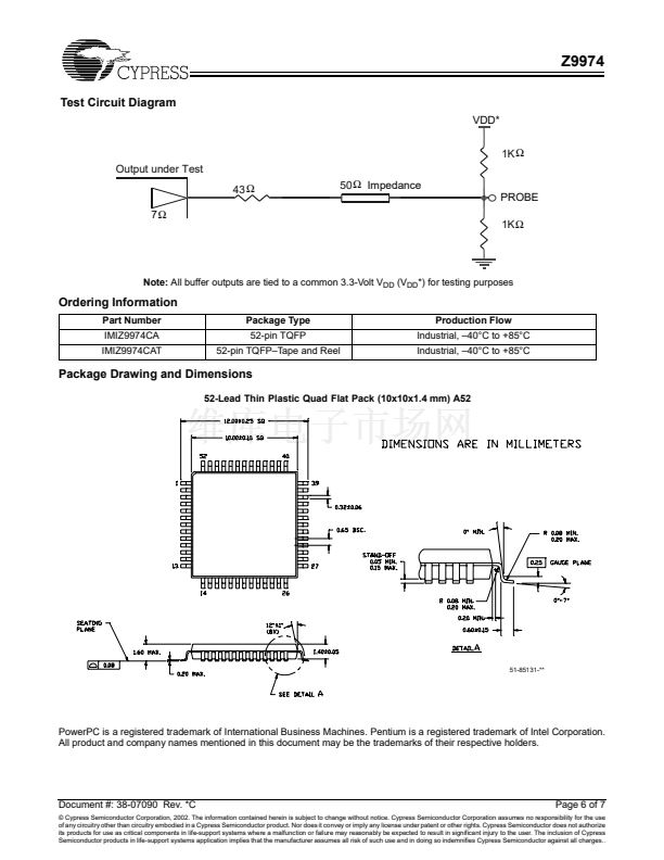
鈥?/div>
Output Frequency up to 125 MHz
Supports PowerPC
廬
, and Pentium
廬
processors
15 Clock outputs: frequency configurable
Two Reference clock inputs for dynamic toggling
Output Three-State control
Spread spectrum compatible
3.3V power supply
Pin compatible with MPC974
Industrial temperature range: 鈥?0擄C to +85擄C
52-pin TQFP package
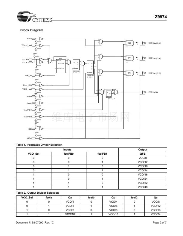
The Z9974 integrates PLL technology for zero delay propaga-
tion from input to output. The PLL feedback is externally avail-
able for propagation delay tuning and divide ratio alternatives
as per
Table 1.
The Z9974 has three banks of outputs with independent divid-
er stages. These dividers allow the banks to have different
frequencies as per
Table 2.
TCLK0 and TCLK1 are selectable input reference clocks and
may be toggled dynamically during operation to provide mod-
ulation and phase shifting designs.
This device includes a Master Reset signal, which disables the
outputs (Hi-Z) mode, and reset all internal digital circuitry (ex-
cluding the PLL).
An Output Enable, OE, input pin is available for disabling the
Qa(0:4), Qb(0:4), and Qc(0:3) outputs and forcing them to
LOW state. All outputs are held LOW with input clock turned
off.
Description
The Z9974 is a low-cost 3.3V zero delay clock driver for
high-speed signal buffering and redistribution.
The designer can select various Input/Output Frequency by
setting fsela, fselb, fselc, fselFB(0:1), and VCO_Sel.
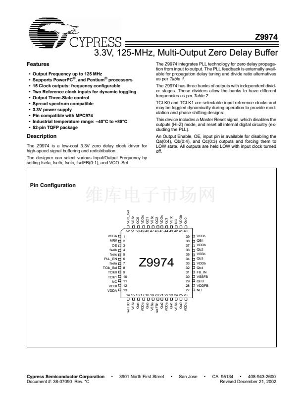
Pin Configuration
VCO_Sel
VSSc
QC0
52 51 50 49 48 47 46 45 44 43 42 41 40
VSSA
MR#
OE
fselb
fselc
PLL_EN
fsela
TClk_Sel
TClk0
TClk1
NC
VDDI
VDDA
1
2
3
4
5
6
7
8
9
10
11
12
13
39
38
37
36
35
34
33
32
31
30
29
28
27
VSSb
QB1
VDDb
Qb2
VSSb
Qb3
VDDb
Qb4
FB_IN
VSSFB
QFB
VDDFB
NC
Z9974
14 15 16 17 18 19 20 21 22 23 24 25 26
VDDa
Qa3
VSSa
selFB1
Qa2
VDDa
Qa1
VSSa
Qa0
VDDa
selFB0
VSSI
Qa4
Cypress Semiconductor Corporation
Document #: 38-07090 Rev. *C
鈥?/div>
3901 North First Street
VDDc
QC1
VSSc
QC2
VDDc
Qc3
VSSc
NC
VDDb
Qb0
鈥?/div>
San Jose
鈥?/div>
CA 95134 鈥?408-943-2600
Revised December 21, 2002


 1
1
 2
2
 3
3
 4
4
 5
5
 6
6
 7
7
