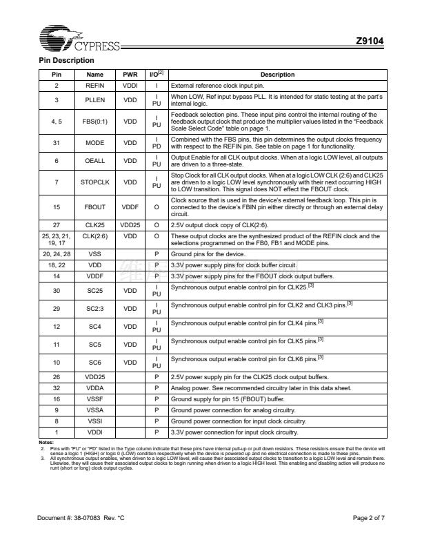
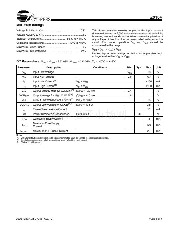
Z9104
Variable Delay Motherboard Clock Buffer
Features
鈥?Output phase relationship is precisely controllable with
respect to input clock via a dedicated external feedback
path
鈥?Two-kV ESD protected
鈥?Six low-skew clocks generated
鈥?One 2.5V output clock
鈥?Outputs are individually enabled
鈥?Output frequencies from 30 to 120 MHz
鈥?3.3V power supply
鈥?Synchronous output enable and disable control
鈥?45鈥?5% output duty cycle
鈥?鹵100 ps cycle-to-cycle jitter
鈥?32-lead TQFP package
鈥?Pin-compatible with MPC932P
Table 1. Feedback Scale Select Codes
Mode
0
0
0
0
1
1
1
1
FBS1 FBS0
0
0
1
1
0
0
1
1
0
1
0
1
0
1
0
1
Pcounter
魯4
魯4
魯4
魯8
魯4
魯4
魯4
魯8
Ncounter
魯8
魯 10
魯 12
魯 12
魯4
魯5
魯6
魯8
MF
[1]
2.0
2.5
3.0
1.5
1.0
1.25
1.5
1.0
Note:
1. Multiplication Factor 鈥?The multiplication factor for these configurations is
the output frequency with respect to REFIN (FOUT = FIN 脳 multiplication
factor).
Block Diagram
MODE
FBS0
FBS1
VDDF
Pin Configuration
FBIN
REFIN
PLLEN
Ncounter
PLL
1
0
FBOUT
Pcounter
VDDI
REFIN
PLLEN
FBS0
FBS1
OEALL
STOPCLK
VSSI
1
2
3
4
5
6
7
8
32
31
30
29
28
27
26
25
24
23
22
21
20
19
18
17
VDDA
MODE
SC25
SC2,3
VSS
CLK25
VDD25
CLK2
SC25
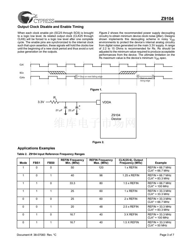
Stop
Logic
Stop
Logic
Stop
Logic
Stop
Logic
Stop
Logic
STOPCLK
OEALL
CLK25
VDD25
Z9104
9
10
11
12
13
14
15
16
CLK2
SC2,3
CLK3
CLK4
CLK5
VSS
CLK3
VDD
CLK4
VSS
CLK5
VDD
CLK6
SC4
SC5
CLK6
VDD
SC6
Cypress Semiconductor Corporation
Document #: 38-07083 Rev. *C
鈥?/div>
3901 North First Street
鈥?/div>
San Jose
VSSA
SC6
SC5
SC4
FBIN
VDDF
FBOUT
VSSF
鈥?/div>
CA 95134
鈥?408-943-2600
Revised May 6, 2002


 1
1
 2
2
 3
3
 4
4
 5
5
 6
6
 7
7
