SC660E
SMBus System Clock Buffer for Mobile Applications
Product Features
摟
摟
摟
摟
摟
摟
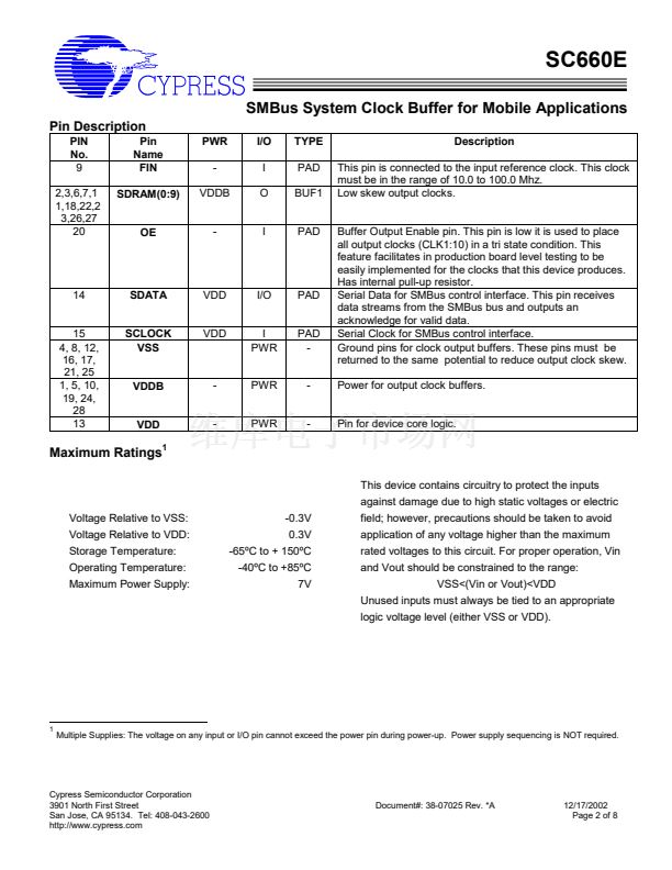
10 output buffers for high clock fanout applications
Each output can be internally disabled for EMI and
power consumption reduction.
Separate power supply for each group of 2 clock
outputs for mixed voltage application.
< 250ps skew between output clocks.
28-pin SSOP package for minimum board space
Single output Tristate pin for testability
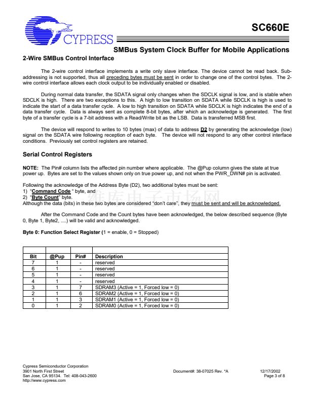
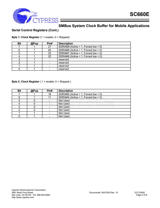
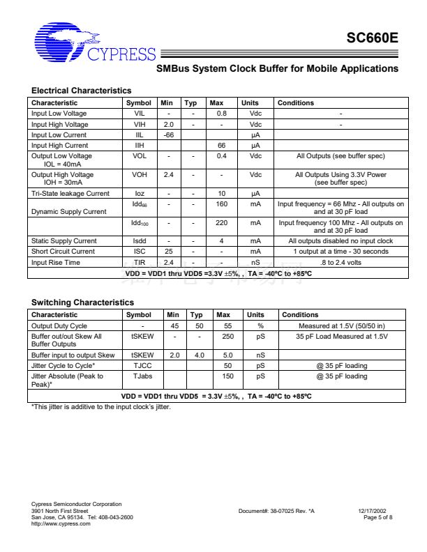
Product Description
The device is a high fanout system clock distributor. Its
primary application is to create the large quantity of
clocks needed to support a wide range of clock loads
that are referenced to a single existing clock. Loads of
up to 30 pF are supported. Primary application of this
component is where long traces are used to transport
clocks from their generating devices to their loads. The
creation of EMI and the degradation of waveform rise
and fall times is greatly reduced by running a single
reference clock trace to this device and then using it to
regenerate the clock that drives shorter traces by using
the SC660 to generate the clocks at the target devices
EMI is therefore minimized and board real estate is
saved.
Block Diagram
VDDB
Pin Configuration
SDRAM(0:1)
SDRAM(2:3)
SDRAM4
FIN
SDRAM5
VDD
SDATA
SCLOCK
OE
I2C
SDRAM(6:7)
SDRAM(8:9)
VDDB
SDRAM0
SDRAM1
VSS
VDDB
SDRAM2
SDRAM3
VSS
FIN
VDDB
SDRAM4
VSS
VDD
SDATA
1
2
3
4
5
6
7
8
9
10
11
12
13
14
28
27
26
25
24
23
22
21
20
19
18
17
16
15
VDDB
SDRAM9
SDRAM8
VSS
VDDB
SDRAM7
SDRAM6
VSS
OE
VDDB
SDRAM5
VSS
VSS
SCLOCK
Cypress Semiconductor Corporation
3901 North First Street
San Jose, CA 95134. Tel: 408-043-2600
http://www.cypress.com
Document#: 38-07025 Rev. *A
12/17/2002
Page 1 of 8


 1
1
 2
2
 3
3
 4
4
 5
5
 6
6
 7
7
 8
8
