鈥?Handles high transient current spikes without saturation.
鈥?Ultra low buzz noise, due to composite construction.
鈥?100% Lead (Pb)-free and RoHS compliant.
鈥?/div>
PDA/Notebook/Desktop/Server applications.
鈥?High current POL converters.
鈥?Low profile, high current power supplies.
鈥?Battery powered devices.
鈥?DC/DC converters in distributed power systems.
鈥?DC/DC converter for Field Programmable Gate Array (FPGA).
DIMENSIONS
in inches [millimeters]
Typical Pad Layout (Min.)
0.255
鹵
0.010
[6.47
鹵
0.254]
0.125
鹵
0.01
[3.18
鹵
0.3]
0.135
[3.43]
0.146
[3.71]
0.290
[7.37]
0.270
鹵
0.015
[6.86
鹵
0.381]
NOTES:
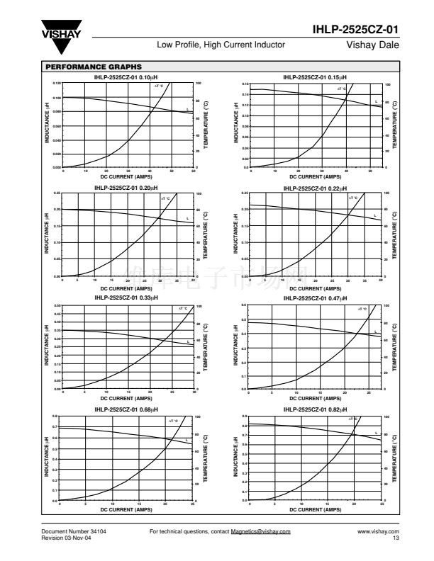
1. All test data is referenced to 25擄C ambient.
2. Operating Temperature Range - 55擄C to + 125擄C
3. DC current (A) that will cause an approximate
鈭員
of 40擄C.
4. DC current (A) that will cause Lo to drop approximately 20%
5. The part temperature (ambient + temp rise) should not exceed
125擄C under worst case operating conditions. Circuit design,
component placement, PWB trace size and thickness, airflow
and other cooling provisions all affect the part temperature. Part
temperature should be verified in the end application.
0.118 [3.0] Max.
0.050
鹵
0.012
[1.27
鹵
0.30]
DESCRIPTION
IHLP-2525CZ-01
MODEL
1.0
碌
H
INDUCTANCE
VALUE
鹵
20%
INDUCTANCE
TOLERANCE
ER
PACKAGE
CODE
e3
JDEC LEAD FREE
STANDARD
GLOBAL PART NUMBER
I
H
L
P
2
5
2
SIZE
5
C
Z
E
R
1
R
0
M
INDUCTANCE
TOLERANCE
0
1
SERIES
MODEL
PACKAGE
CODE
INDUCTANCE
VALUE
See the end of this data book for conversion tables
www.vishay.com
12
For technical questions, contact Magnetics@vishay.com
Document Number 34104
Revision 03-Nov-04


 1
1
 2
2
 3
3
