鈥?/div>
Ideally suited for DDR2 DIMM registered applications
SSTU32864 is optimized for DDR2 Raw Cards B and C R-DIMMs
SSTU32864A is optimized for DDR2 Raw Card A R-DIMMs
Along with CSPU877, zero delay PLL clock buffer, provides
complete solution for DDR2 DIMMs
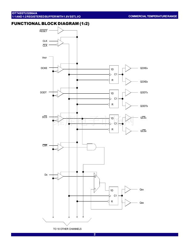
The SSTU32864/A is a 25-bit 1:1 / 14-bit 1:2 configurable registered
buffer designed for 1.7V to 1.9V V
DD
operation. All clock and data inputs
are compatible with the JEDEC standard for SSTL_18. The control inputs
are LVCMOS. All outputs are 1.8V CMOS drivers that have been optimized
to drive the DDR2 DIMM load.
The SSTU32864/A operates from a differential clock (CLK and
CLK).
Data are registered at the crossing of CLK going high and
CLK
going low.
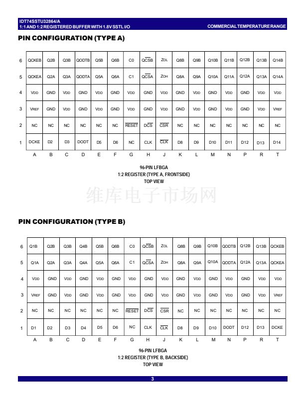
The C0 input controls the pinout configuration of the 1:2 pinout from the
A configuration (when low) to B configuration (when high). The C1 input
controls the configuration from the 25-bit 1:1 (when low) to 14-bit 1:2 (when
high).
This device supports low-power standby operation. When the reset input
(RESET) is low, the differential input receivers are disabled, and undriven
(floating) data, clock, and reference voltage (V
REF
) inputs are allowed. In
addition, when
RESET
is low all registers are reset, and all outputs are
forced low. The LVCMOS
RESET
and Cx inputs must always be held at
a valid logic high or low level.
To ensure defined outputs from the register before a stable clock has
been supplied,
RESET
must be held in the low state during power up.
In the DDR2 DIMM application,
RESET
is specified to be completely
asynchronous with respect to CLK and
CLK.
Therefore, no timing
relationship can be guaranteed between the two. When entering reset, the
register will be cleared and the outputs will be driven low quickly, relative
to the time to disable the differential input receivers. However, when coming
out of a reset, the register will become active quickly, relative to the time to
enable the differential input receivers. As long as the data inputs are low,
and the clock is stable during the time from the low-to-high transition of
RESET
until the input receivers are fully enabled, the design of the
SSTU32864/A must ensure that the outputs will remain low, thus ensuring
no glitches on the outputs.
The device monitors both DCS and
CSR
inputs and will gate the outputs
from changing states when both DCS and
CSR
inputs are high. If either
DCS or
CSR
input is low, the device will function normally. The
RESET
input has priority over the DCS control and will force the inputs low. If the
DCS control functionality is not desired, then the
CSR
input can be hard-
wired to ground, in which case the set-up time requirement for DCS would
be the same as for the other D data inputs.
DESCRIPTION:
COMMERCIAL TEMPERATURE RANGE
1
c
2003 Integrated Device Technology, Inc.
The IDT logo is a registered trademark of Integrated Device Technology, Inc.
AUGUST 2003
DSC-5980/17


 1
1
 2
2
 3
3
 4
4
 5
5
 6
6
 7
7
 8
8
 9
9
 10
10
 11
11
 12
12
