鈥?/div>
Typical
t
SK(0)
(Output Skew) < 250ps
ESD > 2000V per MIL-STD-883, Method 3015;
> 200V using machine model (C = 200pF, R = 0)
V
CC
= 3.3V 鹵0.3V, Normal Range
V
CC
= 2.7V to 3.6V, Extended Range
CMOS power levels (0.4碌 W typ. static)
All inputs, outputs and I/O are 5 Volt tolerant
Supports hot insertion
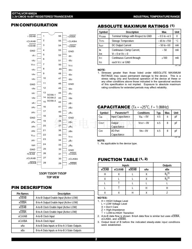
IDT74LVCR16952A
DESCRIPTION:
This 16-bit registered transceiver is built using advanced dual metal
CMOS technology. This high-speed, low power device is organized as two
independent 8-bit D-type registered transceivers with separate input and
output control for independent control of data flow in either direction. For
example, the A-to-B Enable (CEAB) must be LOW to enter data from the A
port. CLKAB controls the clocking function. When CLKAB toggles from LOW-
to-HIGH, the data present on the A port will be clocked into the register.
OEAB
performs the output enable function on the B port. Data flow from the
B port to A port is similar but requires using
CEBA,
CLKBA, and
OEBA
inputs.
Full 16-bit operation is achieved by tying the control pins of the independent
transceivers together.
All pins can be driven from either 3.3V or 5V devices. This feature allows
the use of this device as a translator in a mixed 3.3V/5V supply system.
Drive Features for LVC162952A:
鈥?Balanced Output Drivers: 鹵12mA
鈥?Low Switching Noise
APPLICATIONS:
鈥?5V and 3.3V mixed voltage systems
鈥?Data communication and telecommunication systems
The LVCR162952A has series resistors in the device output structure
which will significantly reduce line noise when used with light loads.This
driver has been developed to drive 鹵12mA at the designated threshold
levels.
FUNCTIONAL BLOCK DIAGRAM
54
1
CEBA
1
CLKBA
1
OEAB
3
1
CEAB
1
CLKAB
2
2
CEAB
2
CLKAB
27
55
1
2
OEAB
26
2
CEBA
2
CLKBA
30
28
31
1
OEBA
56
29
2
OEBA
C
1
A
1
5
CE
D
C
CE
D
52
2
A
1
1
B
1
15
C
CE
D
C
CE
D
42
2
B
1
TO SEVEN OTHER CHANNELS
TO SEVEN OTHER CHANNELS
INDUSTRIAL TEMPERATURE RANGE
1
c
1999 Integrated Device Technology, Inc.
SEPTEMBER 2000
DSC-4484/-


 1
1
 2
2
 3
3
 4
4
 5
5
 6
6
