鈥?/div>
Typical
t
SK(0)
(Output Skew) < 250ps
ESD > 2000V per MIL-STD-883, Method 3015;
> 200V using machine model (C = 200pF, R = 0)
0.635mm pitch SSOP, 0.50mm pitch TSSOP
and 0.40mm pitch TVSOP packages
Extended commercial range of -40擄C to +85擄C
V
CC
= 3.3V 鹵0.3V, Normal Range
V
CC
= 2.7V to 3.6V, Extended Range
CMOS power levels (0.4碌 W typ. static)
All inputs, outputs and I/O are 5 Volt tolerant
Supports hot insertion
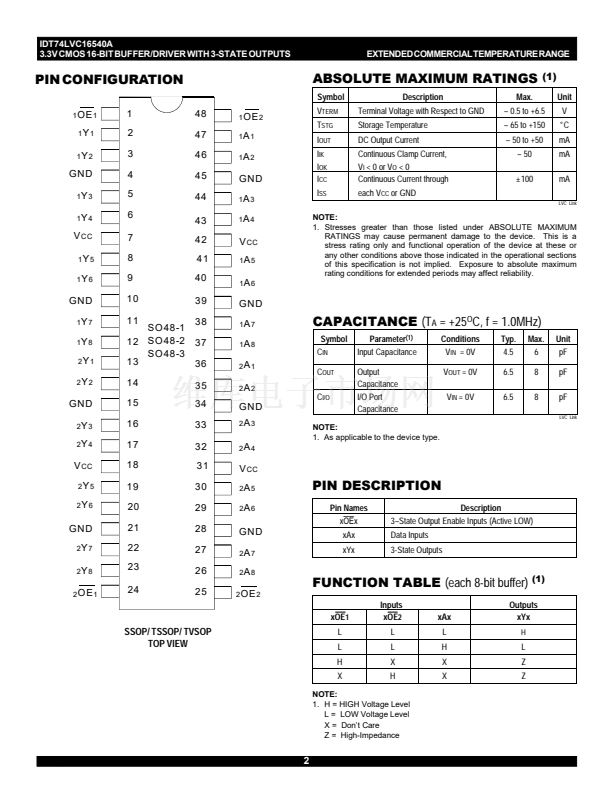
IDT74LVC16540A
DESCRIPTION:
This 16-bit buffer driver is built using advanced dual metal CMOS
technology. The 3-state control gate is a 2-input AND gate with active-low
inputs so that if either output-enable (OE1 or
OE2)
input is high, all
corresponding outputs are in the high-impedance state. To ensure the high-
impedance state during power up or power down,
OE
should be tied to Vcc
through a pullup resistor; the minimum value of the resistor is determined
by the current-sinking capabiltiy of the driver.
All pins of this 16-bit buffer/line driver can be driven from either 3.3V or
5V devices. This feature allows the use of this device as a translator in a
mixed 3.3V/5V supply system.
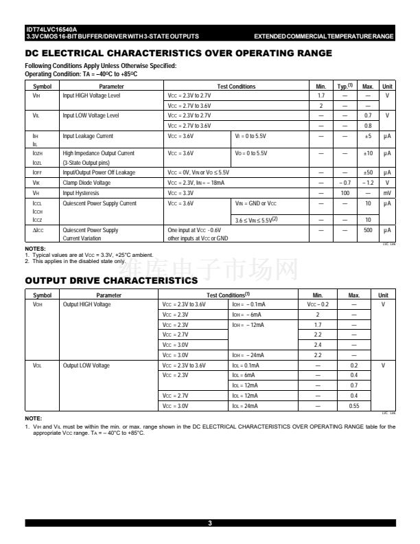
The LVC16540A has been designed with a 鹵24mA output driver. The
driver is capable of driving a moderate to heavy load while maintaining
speed performance.
Drive Features for LVC16540A:
鈥?High Output Drivers: 鹵24mA
鈥?Reduced system switching noise
APPLICATIONS:
鈥?5V and 3.3V mixed voltage systems
鈥?Data communication and telecommunication systems
FUNCTIONAL BLOCK DIAGRAM
1
OE
1
1
OE
2
1
48
2
OE
1
2
OE
2
24
25
1
A
1
47
2
1
Y
1
2
A
1
36
13
2
Y
1
TO SEVEN O TH ER CH ANN ELS
TO SEVEN OTHER CH ANN ELS
EXTENDED COMMERCIAL TEMPERATURE RANGE
1
c
1999 Integrated Device Technology, Inc.
OCTOBER 1999
DSC-4700/-


 1
1
 2
2
 3
3
 4
4
 5
5
 6
6
