FST1632xxx 鈥?28鈩?/div>
鈥?TTL-compatible input and output levels
鈥?ESD > 2000V per MIL-STD-883, Method 3015;
> 200V using machine model (C = 200pF, R = 0)
鈥?Available in SSOP, TSSOP and TVSOP
DESCRIPTION:
The FST163383/1632383 belong to IDT's family of Bus
switches. Bus switch devices perform the function of connect-
ing or isolating two ports without providing any inherent
current sink or source capability. Thus they generate little or
no noise of their own while providing a low resistance path for
an external driver. These devices connect input and output
ports through an n-channel FET. When the gate-to-source
junction of this FET is adequately forward-biased the device
conducts and the resistance between input and output ports
is small. Without adequate bias on the gate-to-source junction
of the FET, the FET is turned off, therefore with no V
CC
applied, the device has hot insertion capability.
The low on-resistance and simplicity of the connection
between input and output ports reduces the delay in this path
to close to zero.
The FST1632xxx integrates terminating resistors in the
device, thus eliminating the need for external 25鈩?series
resistors.
The FST163383 and FST1632383 each provide four 4-bit
TTL- compatible ports that support 2 way bus exchange. The
BX pin controls the bus exchange and the BE pin serves as the
enable pin.
FUNCTIONAL BLOCK DIAGRAM
A
0
C
0
A
5
C
5
B
0
D
0
B
5
D
5
A
4
C
4
A
9
C
9
B
4
B
X1
BE
1
D
4
B
9
B
X2
BE
2
D
9
3474 drw 01
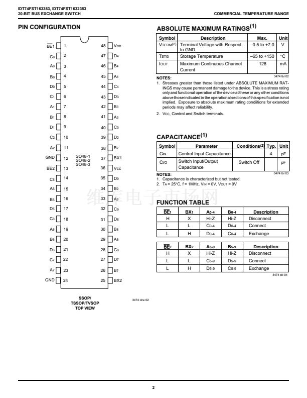
PIN DESCRIPTION
Pin Names
A
0-9
, B
0-9
C
0-9
, D
0-9
I/O
I/O
I/O
I
I
Description
Buses A, B
Buses C, D
Bus Switch Enable (Active LOW)
Bus Exchange
3474 tbl 01
BE
1,2
BX
1,2
The IDT logo is a registered trademark of Integrated Device Technology, Inc.
COMMERCIAL TEMPERATURE RANGE
漏1997
Integrated Device Technology, Inc.
MAY 1996
DSC-3474/4
1


 1
1
 2
2
 3
3
 4
4
 5
5
 6
6
