鈭?/div>
Pin-Out Compatible with Standard 鈥?26 Logic Products
5鈩?A/B bi-directional switch
Isolation Under Power-Off Conditions
Over-voltage tolerant
Latch-up performance exceeds 100mA
V
CC
= 2.3V - 3.6V, normal range
ESD > 2000V per MIL-STD-883, Method 3015;
> 200V using machine model (C = 200pF, R = 0)
Output Enable, Active High
Available in TSSOP and QSOP packages
DESCRIPTION:
The CBTLV3126 features four independent switches. Each switch is
enabled when the associated output-enable (OE) input is high.
To ensure the high-impedance state during power up or power down,
OE should be tied to GND through a pulldown resistor; the minimum value
of the resistor is determined by the current-sinking capability of the driver.
APPLICATIONS:
鈭?/div>
3.3V High Speed Bus Switching and Bus Isolation
FUNCTIONAL BLOCK DIAGRAM
1A
2
SW
SIMPLIFIED SCHEMATIC, EACH
SWITCH
1B
3
1OE
1
2A
5
SW
6
2B
2OE
4
A
B
3A
9
SW
8
3B
3OE
10
4A
12
SW
11
OE
4B
4OE
4
NOTE:
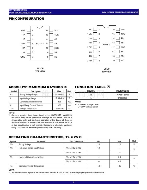
1. Pin numbers shown apply to the 14-pin TSSOP package.
The IDT logo is a registered trademark of Integrated Device Technology, Inc.
INDUSTRIAL TEMPERATURE RANGE
1
c
2001
Integrated Device Technology, Inc.
MARCH 2001
DSC-5740/2


 1
1
 2
2
 3
3
 4
4
 5
5
