鈥?/div>
0.5 MICRON CMOS Technology
Typical t
SK
(o) (Output Skew) < 250ps
ESD > 2000V per MIL-STD-883, Method 3015;
> 200V using machine model (C = 200pF, R = 0)
V
CC
= 3.3V 鹵0.3V, Normal Range
V
CC
= 2.7V to 3.6V, Extended Range
V
CC
= 2.5V 鹵0.2V
CMOS power levels (0.4碌 W typ. static)
Rail-to-Rail output swing for increased noise margin
Available in SOIC, SSOP, QSOP, and TSSOP packages
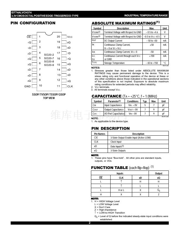
IDT74ALVCH374
DESCRIPTION:
This octal postive edge-triggered D-type flip-flop is built using advanced
dual metal CMOS technology. The ALVCH374 device is particularly
suitable for implementing buffer registers, I/O ports, bidirectional bus drivers,
and working registers. On the positive transition of the clock (CLK) input, the
Q outputs are set to the logic levels at the data (D) inputs.
A buffered output-enable (OE) input can be used to place the eight outputs
in either a normal logic state (high or low logic levels) or a high-impedance
state. In the high-impedance state, the outputs neither load nor drive the bus
lines significantly. The high-impedance state and increased drive provide
the capability to drive bus lines without interface or pullup components.
OE
does not affect internal operations of the latch. Old data can be retained or
new data can be entered while the outputs are in the high-impedance state.
The ALVCH374 has been designed with a 鹵24mA output driver. This
driver is capable of driving a moderate to heavy load while maintaining
speed performance.
The ALVCH374 has a 鈥渂us-hold鈥?which retains the inputs鈥?last state
whenever the input bus goes to a high impedance. This prevents floating
inputs and eliminates the need for pull-up/down resistors.
Drive Features for ALVCH374:
鈥?High Output Drivers: 鹵24mA
鈥?Suitable for heavy loads
APPLICATIONS:
鈥?3.3V High Speed Systems
鈥?3.3V and lower voltage computing systems
FUNCTIONAL BLOCK DIAGRAM
OE
1
CLK
11
C1
2
3
1
D
1
D
1
Q
TO SEVEN OTHER CHANNELS
INDUSTRIAL TEMPERATURE RANGE
1
c
1999 Integrated Device Technology, Inc.
MARCH 1999
DSC-4473/-


 1
1
 2
2
 3
3
 4
4
 5
5
 6
6
