鈥?/div>
0.5 MICRON CMOS Technology
Typical t
SK
(o) (Output Skew) < 250ps
ESD > 2000V per MIL-STD-883, Method 3015;
> 200V using machine model (C = 200pF, R = 0)
V
CC
= 3.3V 鹵0.3V, Normal Range
V
CC
= 2.7V to 3.6V, Extended Range
V
CC
= 2.5V 鹵0.2V
CMOS power levels (0.4碌 W typ. static)
Rail-to-Rail output swing for increased noise margin
Available in SOIC, SSOP, QSOP, and TSSOP packages
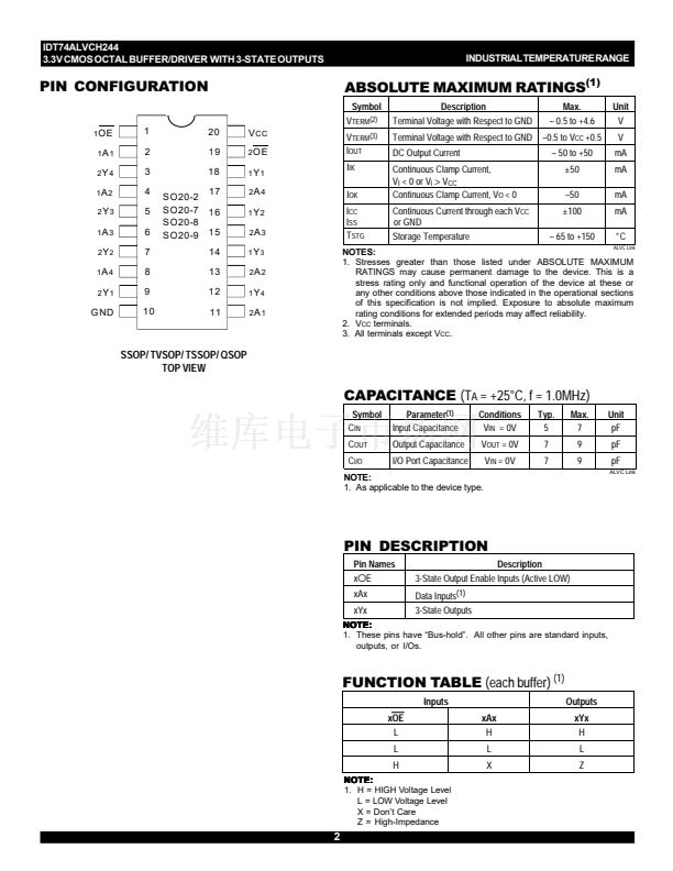
IDT74ALVCH244
DESCRIPTION:
The ALVCH244 octal buffer/driver is built using advanced dual metal
CMOS technology. The ALVCH244 is organized as two 4-bit line drivers
with seperate output-enable (OE) inputs. When
OE
is low, the device passes
data from the A inputs to the Y outputs. When
OE
is high, the outputs are in
the high-impedance state.
To ensure the high-impedance state during power up or power down,
OE
should be tied to V
CC
through a pullup resistor; the minimum value of
the resistor is determined by the current-sinking capability of the driver.
The ALVCH244 has been designed with a 鹵24mA output driver. This
driver is capable of driving a moderate to heavy load while maintaining
speed performance.
The ALVCH244 has a 鈥渂us-hold鈥?which retains the inputs鈥?last state
whenever the input bus goes to a high impedance. This prevents floating
inputs and eliminates the need for pull-up/down resistors.
Drive Features for ALVCH244:
鈥?High Output Drivers: 鹵24mA
鈥?Suitable for heavy loads
APPLICATIONS:
鈥?3.3V High Speed Systems
鈥?3.3V and lower voltage computing systems
FUNCTIONAL BLOCK DIAGRAM
1
1
OE
2
OE
19
1
A
1
2
18
1
Y
1
11
2
A
1
9
2
Y
1
1
A
2
4
16
1
Y
2
13
2
A
2
7
2
Y
2
1
A
3
6
14
1
Y
3
2
A
3
15
5
2
Y
3
1
A
4
8
12
1
Y
4
2
A
4
17
3
2
Y
4
EXTENDED COMMERCIAL TEMPERATURE RANGE
1
c
1999 Integrated Device Technology, Inc.
MARCH 1999
DSC-4472/-


 1
1
 2
2
 3
3
 4
4
 5
5
 6
6
