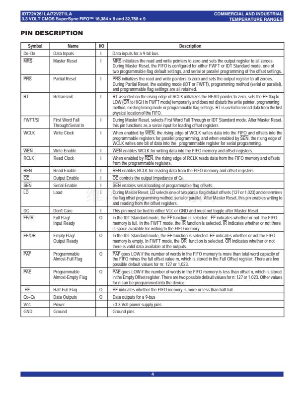
鈥?/div>
Program partial flags by either serial or parallel means
Select IDT Standard timing (using
EF
and
FF
flags) or First
Word Fall Through timing (using
OR
and
IR
flags)
Output enable puts data outputs into high impedance state
Easily expandable in depth and width
Independent Read and Write clocks (permit reading and writing
simultaneously)
Available in the 64-pin Thin Quad Flat Pack (TQFP) and the 64-
pin Slim Thin Quad Flat Pack (STQFP)
High-performance submicron CMOS technology
Industrial temperature range (鈥?0擄C to +85擄C) is available
擄
擄
DESCRIPTION:
The IDT72V261LA/72V271LA are functionally compatible versions of
the IDT72261/72271 designed to run off a 3.3V supply for very low power
consumption. The IDT72V261LA/72V271LA are exceptionally deep, high
speed, CMOS First-In-First-Out (FIFO) memories with clocked read and
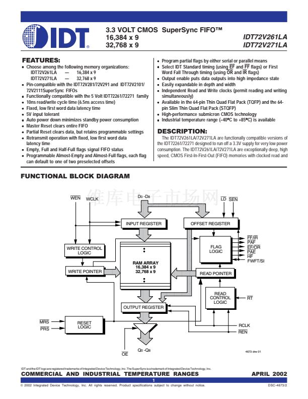
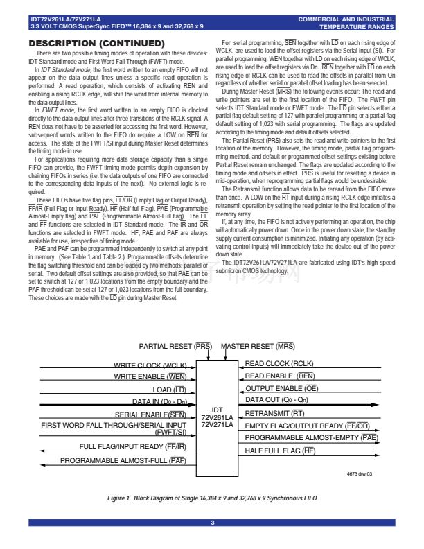
FUNCTIONAL BLOCK DIAGRAM
WEN
D
0
-D
8
WCLK
LD SEN
INPUT REGISTER
OFFSET REGISTER
FF/IR
PAF
EF/OR
PAE
HF
FWFT/SI
WRITE CONTROL
LOGIC
RAM ARRAY
16,384 x 9
32,768 x 9
FLAG
LOGIC
WRITE POINTER
READ POINTER
READ
CONTROL
LOGIC
OUTPUT REGISTER
MRS
PRS
RT
RESET
LOGIC
RCLK
REN
OE
Q
0
-Q
8
4673 drw 01
IDT and the IDT logo are registered trademarks of Integrated Device Technology, Inc. The SuperSync is a trademark of Integrated Device Technology, Inc.
COMMERCIAL AND INDUSTRIAL TEMPERATURE RANGES
1
錚?/div>
2002 Integrated Device Technology, Inc. All rights reserved. Product specifications subject to change without notice.
APRIL 2002
DSC-4673/2


 1
1
 2
2
 3
3
 4
4
 5
5
 6
6
 7
7
 8
8
 9
9
 10
10
 11
11
 12
12
 13
13
 14
14
 15
15
 16
16
 17
17
 18
18
 19
19
 20
20
 21
21
 22
22
 23
23
 24
24
 25
25
 26
26
 27
27
