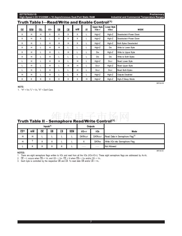
鈼?/div>
Full hardware support of semaphore signaling between
ports on-chip
On-chip port arbitration logic
Fully asynchronous operation from either port
Separate byte controls for multiplexed bus and bus
matching compatibility
Sleep Mode Inputs on both ports
Supports JTAG features compliant to IEEE 1149.1 in
BGA-208 and BGA-256 packages
Single 2.5V (鹵100mV) power supply for core
LVTTL-compatible, selectable 3.3V (鹵150mV)/2.5V (鹵100mV)
power supply for I/Os and control signals on each port
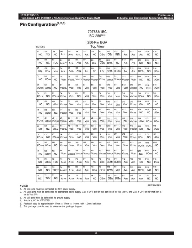
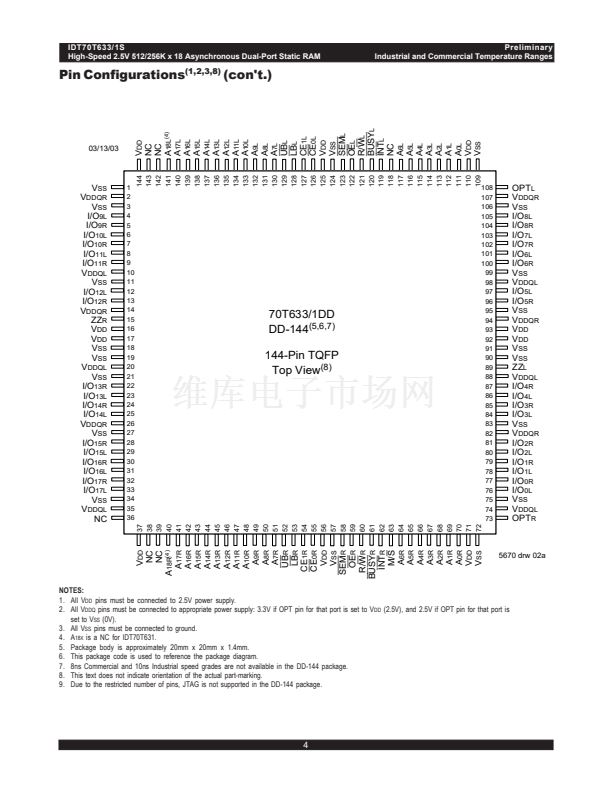
Available in a 256-ball Ball Grid Array, 144-pin Thin Quad
Flatpack and 208-ball fine pitch Ball Grid Array
Industrial temperature range (鈥?0擄C to +85擄C) is available
for selected speeds
UB
R
LB
R
Functional Block Diagram
UB
L
LB
L
R/
W
L
B
E
0
L
B
E
1
L
B
E
1
R
B
E
0
R
R/
W
R
CE
0L
CE
1L
CE
0R
CE
1R
OE
L
Dout0-8_L
Dout9-17_L
Dout0-8_R
Dout9-17_R
OE
R
512/256K x 18
MEMORY
ARRAY
I/O
0L
- I/O
17L
Din_L
Din_R
I/O
0R
- I/O
17R
A
18L
(1)
A
0L
Address
Decoder
ADDR_L
ADDR_R
Address
Decoder
A
18R
(1)
A
0R
TDI
OE
L
CE
0L
CE
1L
ARBITRATION
INTERRUPT
SEMAPHORE
LOGIC
OE
R
CE
0R
CE
1R
TDO
JTAG
TCK
TMS
TRST
R/W
L
R/W
R
BUSY
L(2,3)
SEM
L
INT
L(3)
(4)
BUSY
R(2,3)
M/S
SEM
R
INT
R(3)
NOTES:
LOGIC
1. Address A
18
x is a NC for IDT70T631.
2.
BUSY
is an input as a Slave (M/S=V
IL
) and an output when it is a Master (M/S=V
IH
).
3
BUSY
and
INT
are non-tri-state totem-pole outputs (push-pull).
4. The sleep mode pin shuts off all dynamic inputs, except JTAG inputs, when asserted. OPTx,
INTx,
M/S and the
sleep mode pins themselves (ZZx) are not affected during sleep mode.
ZZ
L
ZZ
CONTROL
ZZ
R
(4)
5670 drw 01
NOVEMBER 2003
DSC-5670/3
1
漏2003 Integrated Device Technology, Inc.


 1
1
 2
2
 3
3
 4
4
 5
5
 6
6
 7
7
 8
8
 9
9
 10
10
 11
11
 12
12
 13
13
 14
14
 15
15
 16
16
 17
17
 18
18
 19
19
 20
20
 21
21
 22
22
 23
23
 24
24
 25
25
 26
26
 27
27
