鈥?/div>
Inputs and outputs are LVTTL (3.3V) compatible
Single 3.3V
鹵
0.3V Power Supply
Single Pulsed RAS interface
SDRAMs have 4 internal banks
Module has 2 physical banks
Fully Synchronous to positive Clock Edge
鈥?Data Mask for Byte Read/Write control
鈥?Programmable Operation:
- CAS Latency: 2, 3
- Burst Type: Sequential or Interleave
- Burst Length: 1, 2, 4, 8, Full-Page (Full-
Page supports Sequential burst only)
- Operation: Burst Read and Write or Multiple
Burst Read with Single Write
鈥?Auto Refresh (CBR) and Self Refresh
鈥?Automatic and controlled Precharge Commands
鈥?Suspend Mode and Power Down Mode
鈥?12/9/2 Addressing (Row/Column/Bank)
鈥?4096 refresh cycles distributed across 64ms
鈥?Serial Presence Detect
鈥?Card size: 2.66" x 1.15" x 0.149"
鈥?Gold contacts
鈥?SDRAM
S
in TSOP Type II Package
Description
IBM13T16644NPA is a 144-pin Synchronous DRAM
Small Outline Dual In-line Memory Module (SO
DIMM) which is organized as a 16Mx64 high-speed
memory array and is configured as two 8Mx64 phys-
ical banks. The SO DIMM uses eight 8Mx16
SDRAMs in 400mil TSOP II packages. The SO
DIMM achieves high speed data transfer rates of up
to 100MHz by employing a prefetch/pipeline hybrid
architecture that supports the JEDEC 1N rule while
allowing very low burst power.
The SO DIMM is intended to comply with all JEDEC
standards set for 144-pin SDRAM SO DIMMs.
All control, address, and data input/output circuits
are synchronized with the positive edge of the exter-
nally supplied clock inputs.
All inputs are sampled at the positive edge of each
externally supplied clock (CK0, CK1). Internal oper-
ating modes are defined by combinations of the
RAS, CAS, WE, S0, S1, DQMB, and CKE0, CKE1
signals. A command decoder initiates the necessary
timings for each operation. A 12-bit address bus
accepts address information in a row/column multi-
plexing arrangement.
Prior to any access operation, the CAS latency,
burst type, burst length, and burst operation type
must be programmed into the SO DIMM by address
inputs A0-A9 during the Mode Register Set cycle.
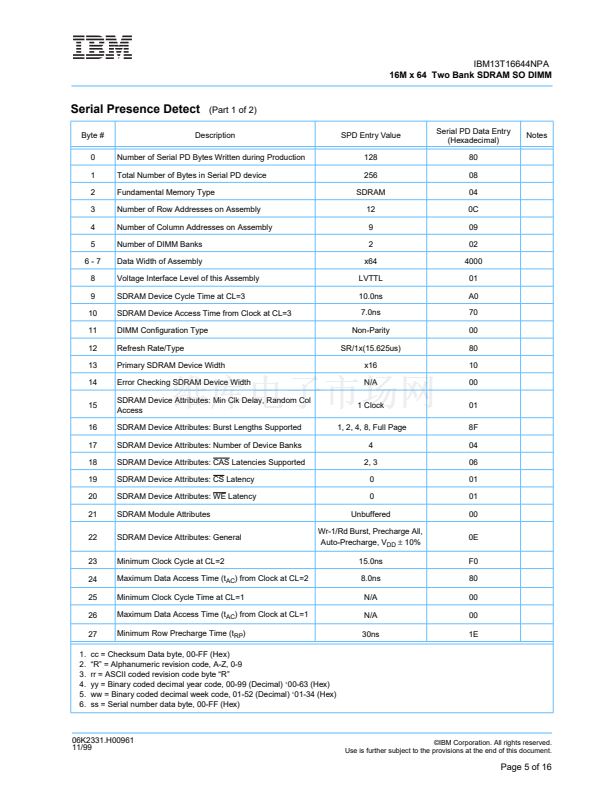
The SO DIMM uses serial presence detects imple-
mented via a serial EEPROM using the two pin IIC
protocol. The first 128 bytes of serial PD data are
used by the DIMM manufacturer. The last 128 bytes
are available to the customer.
All IBM 144-pin SO DIMMs provide a high perfor-
mance, flexible 8-byte interface in a 2.66" long
space-saving footprint.
06K2331.H00961
11/99
漏IBM Corporation. All rights reserved.
Use is further subject to the provisions at the end of this document.
Page 1 of 16


 1
1
 2
2
 3
3
 4
4
 5
5
 6
6
 7
7
 8
8
 9
9
 10
10
 11
11
 12
12
 13
13
 14
14
 15
15
 16
16
