鈥?/div>
Intended for 100MHz and 133MHz applications
Inputs and outputs are LVTTL (3.3V) compatible
Single 3.3V
鹵
0.3V power supply
Single Pulsed RAS interface
SDRAMs have four internal banks
Module has one physical bank
鈥?Fully synchronous to positive clock edge
鈥?Programmable operation:
- DIMM CAS Latency: 4 (Registered mode);
- Burst Type: Sequential or Interleave
- Burst Length: 1, 2, 4, 8, and Full-Page
- Operation: Burst Read and Write or Multiple
Burst Read with Single Write
鈥?Data Mask for Byte Read/Write control
鈥?Auto Refresh (CBR) and Self Refresh
鈥?Automatic and controlled Precharge commands
鈥?Suspend mode and Power Down mode
鈥?12/11/2 Addressing (Row/Column/Bank)
鈥?4096 refresh cycles distributed across 64ms
鈥?Card size: 5.25" x 1.70" x 0.157"
鈥?Gold contacts
鈥?DRAMs in TSOP - Type II Package
鈥?Serial Presence Detect with Write protect
Description
IBM13M32734CCB is a registered 168-Pin Syn-
chronous DRAM Dual In-Line Memory Module
(DIMM) organized as a 32Mx72 high-speed mem-
ory array. The DIMM uses 18 32Mx4 SDRAMs in
400 mil TSOP packages. The DIMM achieves high-
speed data-transfer rates of 100MHz and 133MHz
by employing a prefetch/pipeline hybrid architecture
that synchronizes the output data to a system clock.
The DIMM is intended for use in applications oper-
ating at 100MHz and 133MHz memory bus speeds.
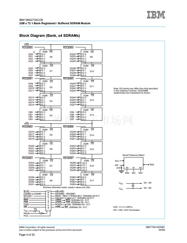
All control and address signals are re-driven
through registers/buffers to the SDRAM devices.
Operating in registered mode (REGE pin tied high),
the control/address input signals are latched in the
register on one rising clock edge and sent to the
SDRAM devices on the following rising clock edge
(data access is delayed by one clock).
A phase-lock loop (PLL) on the DIMM is used to re-
drive the clock signals to both the SDRAM devices
and the registers to minimize system clock loading.
(CK0 is connected to the PLL, and CK1, CK2, and
CK3 are terminated on the DIMM). A single clock
enable (CKE0) controls all devices on the DIMM,
enabling the use of SDRAM Power Down modes.
Prior to any access operation, the device CAS
latency and burst type/length/operation type must
be programmed into the DIMM by address inputs
A0-A10 using the mode register set cycle. The
DIMM CAS latency when operated in Registered
mode is one clock later than the device CAS latency
due to the address and control signals being
clocked to the SDRAM devices.
The DIMM uses serial presence detects imple-
mented via a serial EEPROM using the two-pin IIC
protocol. The first 128 bytes of serial PD data are
programmed and locked by the DIMM manufac-
turer. The last 128 bytes are available to the cus-
tomer and may be write protected by providing a
high level to pin 81 on the DIMM. An on-board pull-
down resistor keeps this in the Write Enable mode.
All IBM 168-pin DIMMs provide a high-performance,
flexible 8-byte interface in a 5.25" long space-saving
footprint.
06K7740.H03381
04/00
漏IBM Corporation. All rights reserved.
Use is further subject to the provisions at the end of this document.
Page 1 of 20


 1
1
 2
2
 3
3
 4
4
 5
5
 6
6
 7
7
 8
8
 9
9
 10
10
 11
11
 12
12
 13
13
 14
14
 15
15
 16
16
 17
17
 18
18
 19
19
 20
20
