HY5W2A2(L/S)F / HY57W2A3220(L/S)T
HY5W22F / HY57W283220T
4Banks x 1M x 32bits Synchronous DRAM
DESCRIPTION
The Hynix Low Power SDRAM is suited for non-PC application which use the batteries such as PDAs, 2.5G and 3G
cellular phones with internet access and multimedia capabilities, mini-notebook, handheld PCs
The Hynix HY5W2A2F series is a 134,217,728-bit CMOS Synchronous DRAM, ideally suited for the memory applica-
tions which require wide data I/O and high bandwidth. HY5W2A2F series is organized as 4banks of 1,048,576x32.
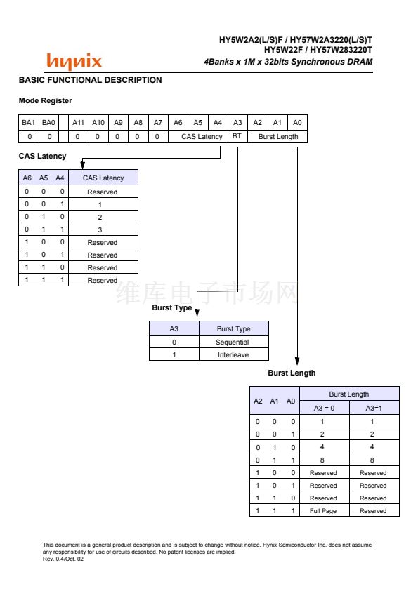
The Low Power SDRAM provides for programmable options including CAS latency of 1, 2, or 3, READ or WRITE burst
length of 1, 2, 4, 8, or full page, and the burst count sequence(sequential or interleave). And the Low Power SDRAM
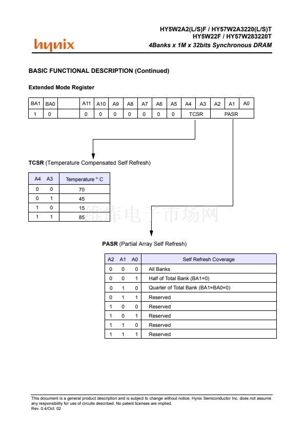
also provides for special programmable options including Partial Array Self Refresh of 1bank, 2banks, or all banks,
Temperature Compensated Self Refresh of 15, 45, 70, or 85 degrees C. A burst of Read or Write cycles in progress
can be terminated by a burst terminate command or can be interrupted and replaced by a new burst Read or Write
command on any cycle(This pipelined design is not restricted by a 2N rule).
Deep Power Down Mode is a additional operating mode for Low Power SDRAM. This mode can achieve maximum
power reduction by removing power to the memory array within each SDRAM. By using this feature, the system can
cut off alomost all DRAM power without adding the cost of a power switch and giving up mother-board power-line lay-
out flexibility.
FEATURES
鈥?/div>
鈥?/div>
鈥?/div>
鈥?/div>
鈥?/div>
鈥?/div>
Standard SDRAM Protocol
Internal 4bank operation
Voltage : VDD = 2.5V, VDDQ = 1.8V
& 2.5V
LVTTL compatible I/O Interface
Low Voltage interface to reduce I/O power
Low Power Features ( HY5W22F / HY57W283220T series can鈥檛 support these features)
- PASR(Partial Array Self Refresh)
- TCSR(Temperature Compensated Self Refresh)
- Deep Power Down Mode
Packages : 90ball, 0.8mm pitch FBGA / 86pin, TSOP
-25 ~ 85C Operation
鈥?/div>
鈥?/div>
ORDERING INFORMATION
Part No.
HY57W2A3220(L/S)T-H
HY5W2A2(L/S)F-H
HY57W2A3220(L/S)T-8
HY5W2A2(L/S)F-8
HY57W2A3220(L/S)T-P
HY5W2A2(L/S)F-P
HY57W2A3220(L/S)T-S
HY5W2A2(L/S)F-S
HY57W2A3220(L/S)T-B
HY5W2A2(L/S)F-B
Clock Frequency
CAS Latench
133MHz
CL 3
125MHz
CL 3
100MHz
CL 2
100MHz
CL 3
66MHz
CL 2
Organization
4Banks x 1Mbits
x32
4Banks x 1Mbits
x32
4Banks x 1Mbits
x32
4Banks x 1Mbits
x32
4Banks x 1Mbits
x32
Interface
LVTTL
LVTTL
LVTTL
LVTTL
LVTTL
Package
90balls FBGA
(HY5xxxxxxF)
86pin TSOP-II
(HY5xxxxxxT)
This document is a general product description and is subject to change without notice. Hynix Semiconductor Inc. does not assume
any responsibility for use of circuits described. No patent licenses are implied.
Rev. 0.4/Oct. 02
HY5W2A2(L/S)F相關型號PDF文件下載
-
型號
版本
描述
廠商
下載
-
英文版
x16 SDRAM
ETC
-
英文版
SDRAM|4X2MX16|CMOS|BGA|54PIN|PLASTIC
ETC
-
英文版
x16 SDRAM
ETC
-
英文版
SDRAM|4X2MX16|CMOS|BGA|54PIN|PLASTIC
ETC
-
英文版
HY5W6B6DLF_Hynix.pdf
Hynix
-
英文版
x16 SDRAM
ETC
-
英文版
SDRAM|4X2MX16|CMOS|BGA|54PIN|PLASTIC
ETC
-
英文版
x16 SDRAM
ETC
-
英文版
SDRAM|4X2MX16|CMOS|BGA|54PIN|PLASTIC
ETC
-
英文版
x16 SDRAM
ETC
-
英文版
SDRAM|4X2MX16|CMOS|BGA|54PIN|PLASTIC
ETC
-
英文版
4Mx32|2.5V|4K|H|Handy SDRAM - 128M
ETC
-
英文版
4Mx32|2.5V|4K|H|Handy SDRAM - 128M
ETC


 1
1
 2
2
 3
3
 4
4
 5
5
 6
6
 7
7
 8
8
 9
9
 10
10
 11
11
 12
12
 13
13
 14
14
 15
15
 16
16
 17
17
 18
18
 19
19
 20
20
 21
21
 22
22
 23
23
 24
24
 25
25
