鈥?/div>
Ideal for 315.0 MHz Automotive Keyless-Entry Transmitters
Quartz SAW Frequency Stabilization and Harmonic Filtering
Compact, Surface-Mount Case with <90 mm
2
Footprint
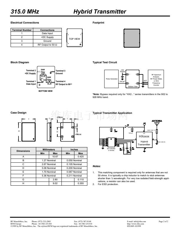
The HX1005 is a miniature transmitter module that generates on-off keyed (OOK) modulation from an exter-
nal digital encoder (not included). The carrier frequency is quartz, surface-acoustic-wave (SAW) stabilized,
and output harmonics are suppressed by a SAW filter. The result is excellent performance in a simple-to-
use, surface-mount device with a low external component count. The HX1005 is designed specifically for
unlicensed remote-control and wireless security transmitters operating at 315.0 MHz in the USA under FCC
Part 15 regulations, in Canada under DOC RSS-210, and in Italy.
315.0 MHz
Hybrid
Transmitter
Absolute Maximum Ratings
Rating
Power Supply and/or Modulation Input Voltage
Nonoperating Case Temperature
Ten-Second Soldering Temperature
Value
10
-40 to +85
230
Units
V
擄C
擄C
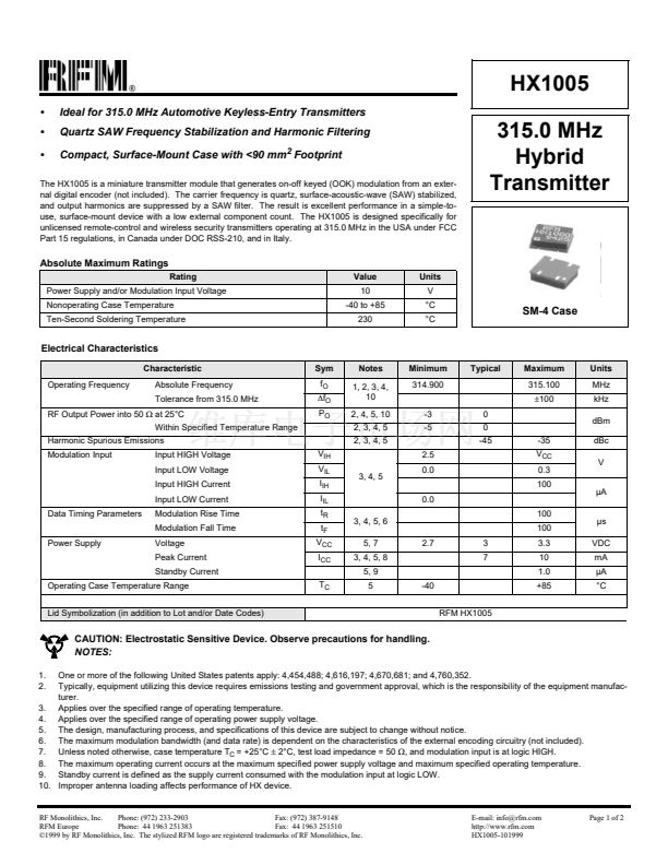
SM-4 Case
Electrical Characteristics
Characteristic
Operating Frequency
Absolute Frequency
Tolerance from 315.0 MHz
RF Output Power into 50
鈩?/div>
at 25擄C
Within Specified Temperature Range
Harmonic Spurious Emissions
Modulation Input
Input HIGH Voltage
Input LOW Voltage
Input HIGH Current
Input LOW Current
Data Timing Parameters
Power Supply
Modulation Rise Time
Modulation Fall Time
Voltage
Peak Current
Standby Current
Operating Case Temperature Range
Lid Symbolization (in addition to Lot and/or Date Codes)
T
C
V
IH
V
IL
I
IH
I
IL
t
R
t
F
V
CC
I
CC
3, 4, 5, 6
5, 7
3, 4, 5, 8
5, 9
5
-40
RFM HX1005
2.7
3
7
3, 4, 5
Sym
f
O
鈭唂
O
P
O
Notes
1, 2, 3, 4,
10
2, 4, 5, 10
2, 3, 4, 5
2, 3, 4, 5
2.5
0.0
0.0
100
100
3.3
10
1.0
+85
Minimum
314.900
-3
-5
0
0
-45
-35
V
CC
0.3
100
Typical
Maximum
315.100
鹵100
Units
MHz
kHz
dBm
dBc
V
碌A(chǔ)
碌s
VDC
mA
碌A(chǔ)
擄C
CAUTION: Electrostatic Sensitive Device. Observe precautions for handling.
NOTES:
One or more of the following United States patents apply: 4,454,488; 4,616,197; 4,670,681; and 4,760,352.
Typically, equipment utilizing this device requires emissions testing and government approval, which is the responsibility of the equipment manufac-
turer.
3. Applies over the specified range of operating temperature.
4. Applies over the specified range of operating power supply voltage.
5. The design, manufacturing process, and specifications of this device are subject to change without notice.
6. The maximum modulation bandwidth (and data rate) is dependent on the characteristics of the external encoding circuitry (not included).
7. Unless noted otherwise, case temperature T
C
= +25擄C
鹵
2擄C, test load impedance = 50
鈩?
and modulation input is at logic HIGH.
8. The maximum operating current occurs at the maximum specified power supply voltage and maximum specified operating temperature.
9. Standby current is defined as the supply current consumed with the modulation input at logic LOW.
10. Improper antenna loading affects performance of HX device.
1.
2.
RF Monolithics, Inc.
Phone: (972) 233-2903
Fax: (972) 387-9148
RFM Europe
Phone: 44 1963 251383
Fax: 44 1963 251510
漏1999 by RF Monolithics, Inc. The stylized RFM logo are registered trademarks of RF Monolithics, Inc.
E-mail: info@rfm.com
http://www.rfm.com
HX1005-101999
Page 1 of 2


 1
1
 2
2
