HUF76112SK8
Data Sheet
December 2001
7.5A, 30V, 0.026 Ohm, N-Channel, Logic
Level Power MOSFET
The HUF76112SK8 is an Application-Specific MOSFET
optimized for switching when used as the upper switch in
synchronous buck applications. The low gate charge and low
input capacitance results in lower driver and lower switching
losses, thereby increasing the overall system efficiency.
Features
鈥?7.5A, 30V
- r
DS(ON)
= 0.026鈩? V
GS
=
10V
- r
DS(ON)
= 0.033鈩? V
GS
=
5V
鈥?PWM Optimized for Synchronous Buck Applications
鈥?Fast Switching
鈥?Low Gate Charge
- Q
g
Total 15nC (Typ)
鈥?Low Capacitance
- C
ISS
725pF (Typ)
- C
RSS
36pF (Typ)
Symbol
SOURCE (1)
SOURCE (2)
SOURCE (3)
GATE (4)
DRAIN (8)
DRAIN (7)
DRAIN (6)
DRAIN (5)
Packaging
SO8 (JEDEC MS-012AA)
BRANDING DASH
Ordering Information
5
PART NUMBER
HUF76112SK8
PACKAGE
MS-012AA
BRAND
76112SK8
1
2
3
4
NOTE: When ordering, use the entire part number. Add the suffix T
to obtain the HUF76112SK8 in tape and reel, e.g., HUF76112SK8T.
T
A
= 25
o
C, Unless Otherwise Specified
PARAMETER
HUF76112SK8
30
30
鹵16
7.5
4.0
Figure 4
2.5
20
-55 to 150
300
260
50
152
189
UNITS
V
V
V
A
A
A
W
mW/
o
C
o
C
o
C
o
C
o
C/W
o
C/W
o
C/W
Absolute Maximum Ratings
SYMBOL
V
DSS
V
DGR
V
GS
I
D
I
D
I
DM
P
D
T
J
, T
STG
T
L
T
pkg
Drain to Source Voltage (Note 1)
Drain to Gate Voltage (R
GS
= 20k鈩? (Note 1)
Gate to Source Voltage
Drain Current
Continuous (T
A
= 25
o
C, V
GS
= 10V) (Figure 2) (Note 2)
Continuous (T
A
= 100
o
C, V
GS
= 5V) (Note 2)
Pulsed Drain Current
Power Dissipation (Note 2)
Derate Above 25
o
C
Operating and Storage Temperature
Maximum Temperature for Soldering
Leads at 0.063in (1.6mm) from Case for 10s
Package Body for 10s, See Techbrief TB334
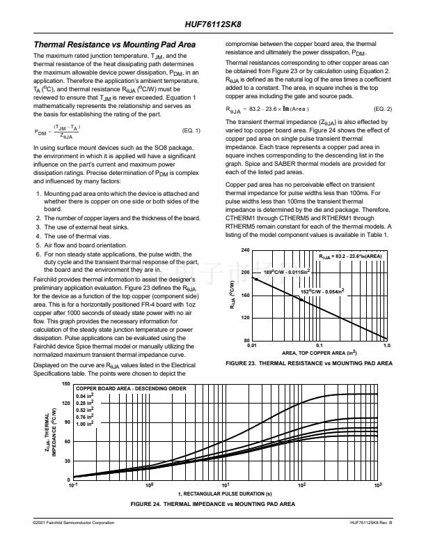
Thermal Resistance Junction to Ambient
Measured using FR-4 board with 0.76 in
2
(490.3 mm
2
) copper pad at 10
second.
THERMAL SPECIFICATIONS
R
胃JA
Measured using FR-4 board with 0.054 in
2
(34.8 mm
2
) copper pad at 1000
seconds. (Figure 23)
Measured using FR-4 board with 0.0115 in
2
(7.42 mm
2
) copper pad at 1000
seconds. (Figure 23)
NOTES:
1. T
J
= 25
o
C to 125
o
C.
2. R
胃JA
= 50
o
C/W
CAUTION:
Stresses above those listed in 鈥淎bsolute Maximum Ratings鈥?may cause permanent damage to the device. This is a stress only rating and operation of the
device at these or any other conditions above those indicated in the operational sections of this specification is not implied.
漏2001 Fairchild Semiconductor Corporation
HUF76112SK8 Rev. B


 1
1
 2
2
 3
3
 4
4
 5
5
 6
6
 7
7
 8
8
 9
9
 10
10
 11
11
