INTERNAL PACKAGE CODE 鈥淗SQ鈥?/div>
TOP VIEW
*GND 1
Q4 2
D4 3
Q5 4
D5 5
A0 6
A1 7
A2 8
E3 9
*W2 10
W2 11
E4 12
A11 13
A10 14
A9 15
D6 16
Q6 17
D7 18
Q7 19
*VDD 20
40 VDD*
39 Q0
38 D0
37 Q1
36 D1
35 A6
34 A7
33 A9
32 E1
31 W1
30 W1*
29 E2
28 A3
27 A2
26 A5
25 D2
24 Q2
23 D3
22 Q3
21 GND*
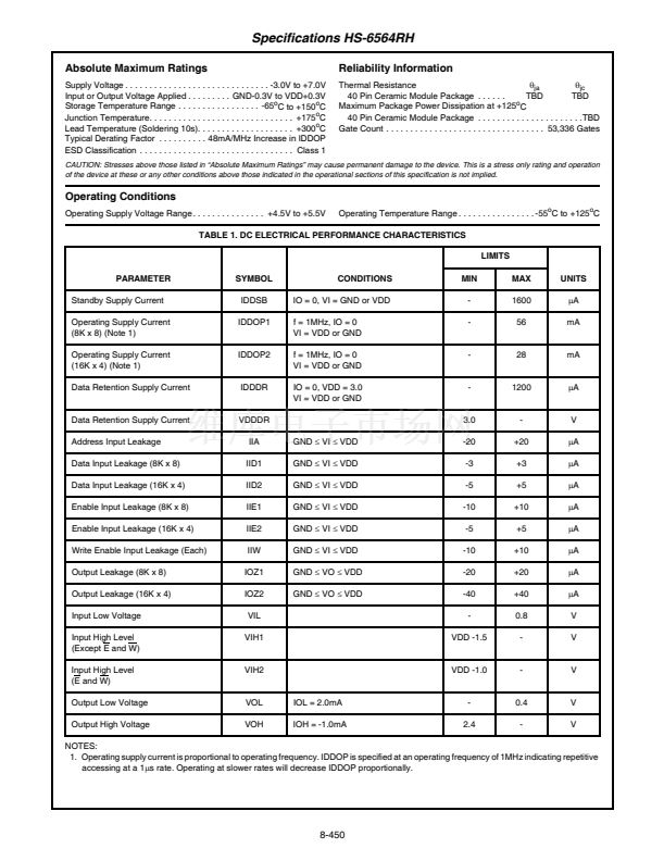
鈥?Radiation Hardened EPI CMOS
- Total Dose 1 x 10
5
RAD (Si)
- Transient Upset > 1 x 10
8
RAD (Si)/s
- Latch-Up Free to > 1 x 10
12
RAD (Si)/s
鈥?Low Power Standby 4.4mW Maximum
鈥?Low Power Operation 308mW/MHz Maximum
鈥?Data Retention 3.0V Minimum
鈥?TTL Compatible In/Out
鈥?Three State Outputs
鈥?Fast Access Time 250ns Maximum
鈥?Military Temperature Range -55
o
C to +125
o
C
鈥?On Chip Address Registers
鈥?Organizable 8K x 8 or 16K x 4
鈥?40 Pin DIP Pinout 2.000" x 0.900"
Description
The HS-6564RH is a radiation hardened 64K bit, synchronous CMOS RAM
module. It consists of 16 HS-6504RH 4K x 1 radiation hardened CMOS RAMs, in
leadless carriers, mounted on a ceramic substrate. The individual RAMs are
fabricated using the Intersil radiation hardened guard ring, self-aligned silicon gate
technology. The HS-6564RH is configured as an extra wide, standard length 40 pin
DIP. The memory appears to the system as an array of 16 4K x 1 static RAMs. The
array is organized as two 8K by 4 blocks of RAM sharing only the address bus. The
data inputs, data outputs, chip enables and write enables are seperate for each
block of RAM. This allows the user to organize the HS-6564RH RAM as either an
8K by 8 or a 16K by 4 array.
This 64K memory provides a unique blend of low power CMOS semiconductor
technology and advanced packaging techniques. The HS-6564RH is intended for
use in radiation environments where a large amount of RAM is needed, and where
power consumption and board space are prime concerns. On-chip latches are
provided for addresses, data input and data output allowing efficient interfacing with
microprocessor systems. The data output can be forced to a high impedance for
use in expanded memory arrays. The guaranteed low voltage data retention
characteristics allow easy implementation of non-volatile readswrite memory by
using very small batteries mounted directly on the memory circuit board.
A
W1
E1
12
* Pins 20 and 40 (VDD) are internally connected.
Similarly pins 1 and 21 (Ground) are connected.
The user is advised to connect both VDD pins
and both Ground pins to the board busses. This
will improve power distribution across the array
and will enhance decoupling.
Pin 10 is internally connected to pin 11, and pin
30 is connected to pin 31. For those users wish-
ing to preserve board compatibility with possible
future RAM arrays, we recommend connections
to the write lines be made at pins 11 and 31,
leaving pins 10 and 30 free for future expansion.
Functional Diagram
A
W
EDQ
E2
D0
W2
E3
Q0
D1
Q1
D2
Q2
D3
Q3
E4
D4
Q4
D5
Q5
D6
Q6
D7
Q7
CAUTION: These devices are sensitive to electrostatic discharge; follow proper IC Handling Procedures.
1-888-INTERSIL or 321-724-7143
|
Intersil (and design) is a registered trademark of Intersil Americas Inc.
Copyright 漏 Intersil Americas Inc. 2002. All Rights Reserved
8-449
File Number
3032.1


 1
1
 2
2
 3
3
 4
4
 5
5
 6
6
 7
7
 8
8
 9
9
