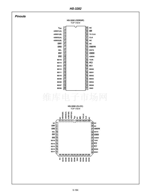
HS-3282
REFERENCE AN400
March 1997
CMOS ARINC Bus Interface Circuit
Description
The HS-3282 is a high performance CMOS bus interface
circuit that is intended to meet the requirements of ARINC
Speci鏗乧ation 429, and similar encoded, time multiplexed
serial data protocols. This device is intended to be used with
the HS-3182, a monolithic Dl bipolar differential line driver
designed to meet the speci鏗乧ations of ARINC 429. The
ARINC 429 bus interface circuit consists of two (2) receivers
and a transmitter operating independently as shown in
Figure 1. The two receivers operate at a frequency that is ten
(10) times the receiver data rate, which can be the same or
different from the transmitter data rate. Although the two
receivers operate at the same frequency, they are
functionally independent and each receives serial data asyn-
chronously. The transmitter section of the ARINC bus
interface circuit consists mainly of a First-In First-Out (FIFO)
memory and timing circuit. The FIFO memory is used to hold
up to eight (8) ARINC data words for transmission serially.
The timing circuit is used to correctly separate each ARINC
word as required by ARINC Speci鏗乧ation 429. Even though
ARINC Speci鏗乧ation 429 speci鏗乪s a 32-bit word, including
parity, the HS-3282 can be programmed to also operate with
a word length of 25 bits. The incoming receiver data word
parity is checked, and a parity status is stored in the receiver
latch and output on Pin BD08 during the 1st word. [A logic
鈥?鈥?indicates that an odd number of logic 鈥?鈥?s were received
and stored; a logic 鈥?鈥?indicates that an even number of logic
鈥?鈥漵 were received and stored]. In the transmitter the parity
generator will generate either odd or even parity depending
upon the status of PARCK control signal. A logic 鈥?鈥?on BD12
will cause odd parity to be used in the output data stream.
Versatility is provided in both the transmitter and receiver by
the external clock input which allows the bus interface circuit
to operate at data rates from 0 to 100 kilobits. The external
clock must be ten (10) times the data rate to insure no data
ambiguity.
The ARINC bus interface circuit is fully guaranteed to
support the data rates of ARINC speci鏗乧ation 429 over both
the voltage (鹵5%) and full military temperature range. It
interfaces with UL, CMOS or NMOS support circuitry, and
uses the standard 5-volt V
CC
supply.
Features
鈥?ARlNC Speci鏗乧ation 429 Compatible
鈥?Data Rates of 100 Kilobits or 12.5 Kilobits
鈥?Separate Receiver and Transmitter Section
鈥?Dual and Independent Receivers, Connecting Directly
to ARINC Bus
鈥?Serial to Parallel Receiver Data Conversion
鈥?Parallel to Serial Transmitter Data Conversion
鈥?Word Lengths of 25 or 32 Bits
鈥?Parity Status of Received Data
鈥?Generate Parity of Transmitter Data
鈥?Automatic Word Gap Timer
鈥?Single 5V Supply
鈥?Low Power Dissipation
鈥?Full Military Temperature Range
Ordering Information
PACKAGE
CERDIP
SMD#
CLCC
-40
o
C to +85
o
C
-55
o
C to +125
o
C
TEMP. RANGE
-55
o
C to +125
o
C
PART NUMBER
HS1-3282-8
5962-8688001QA
HS4-3282-9+
HS4-3282-8
5962-8688001XA
PKG.
NO.
F40.6
F40.6
J44.A
J44.A
J44.A
SMD#
CAUTION: These devices are sensitive to electrostatic discharge; follow proper IC Handling Procedures.
http://www.intersil.com or 407-727-9207
|
Copyright
漏
Intersil Corporation 1999
File Number
2964.2
5-183


 1
1
 2
2
 3
3
 4
4
 5
5
 6
6
 7
7
 8
8
 9
9
 10
10
 11
11
 12
12
 13
13
 14
14
 15
15
