鈥?/div>
SAW Frequency Stabilization
Fundamental-Mode Oscillation at 400.0 MHz
A Rugged, Compact General-Purpose Oscillator
The frequency of this oscillator is stabilized by surface-acoustic-wave (SAW) technology. This results in ex-
cellent performance from a compact, rugged, oscillator operating at the fundamental frequency of 400.0 MHz.
The high-reliability of the HO4002-1 makes it suitable for general purpose use in a wide variety of applications.
Absolute Maximum Ratings
Rating
DC Supply Voltage
Case Temperature
Powered
Storage
Value
0 to +13
-40 to +70
-40 to +85
Units
VDC
擄C
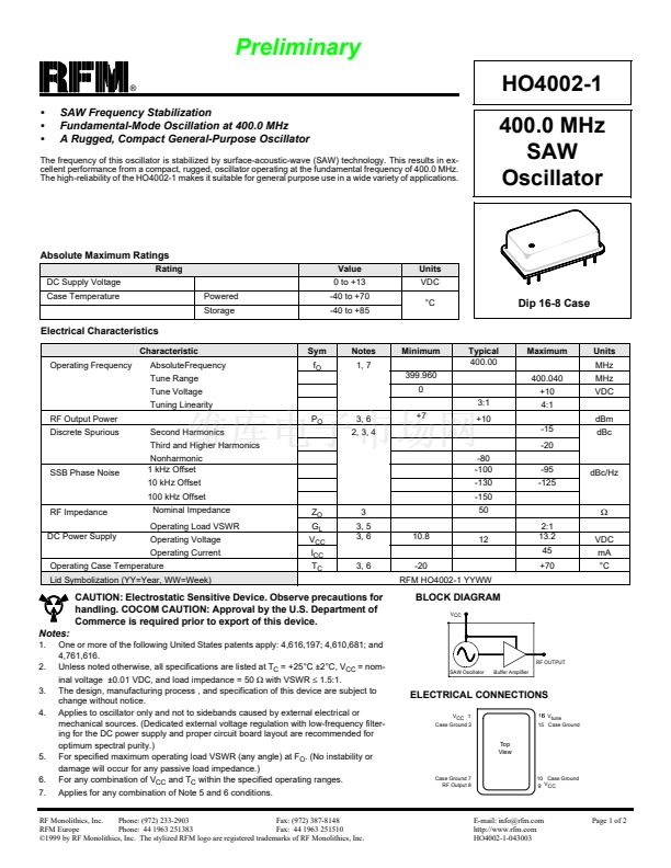
Dip 16-8 Case
Electrical Characteristics
Characteristic
Operating Frequency
AbsoluteFrequency
Tune Range
Tune Voltage
Tuning Linearity
RF Output Power
Discrete Spurious
Second Harmonics
Third and Higher Harmonics
SSB Phase Noise
Nonharmonic
1 kHz Offset
10 kHz Offset
100 kHz Offset
RF Impedance
DC Power Supply
Nominal Impedance
Operating Load VSWR
Operating Voltage
Operating Current
Operating Case Temperature
Lid Symbolization (YY=Year, WW=Week)
Z
O
G
L
V
CC
I
CC
T
C
3, 6
-20
RFM HO4002-1 YYWW
3
3, 5
3, 6
10.8
-80
-100
-130
-150
50
12
2:1
13.2
45
+70
鈩?/div>
VDC
mA
擄C
P
O
3, 6
2, 3, 4
+7
Sym
f
O
Notes
1, 7
399.960
0
3:1
+10
-15
-20
-95
-125
dBc/Hz
Minimum
Typical
400.00
Maximum
400.040
+10
4:1
dBm
dBc
Units
MHz
MHz
VDC
CAUTION: Electrostatic Sensitive Device. Observe precautions for
handling. COCOM CAUTION: Approval by the U.S. Department of
Commerce is required prior to export of this device.
Notes:
1.
2.
3.
4.
One or more of the following United States patents apply: 4,616,197; 4,610,681; and
4,761,616.
Unless noted otherwise, all specifications are listed at T
C
= +25擄C 鹵2擄C, V
CC
= nom-
inal voltage 鹵0.01 VDC, and load impedance = 50
鈩?/div>
with VSWR
鈮?/div>
1.5:1.
The design, manufacturing process , and specification of this device are subject to
change without notice.
Applies to oscillator only and not to sidebands caused by external electrical or
mechanical sources. (Dedicated external voltage regulation with low-frequency filter-
ing for the DC power supply and proper circuit board layout are recommended for
optimum spectral purity.)
For specified maximum operating load VSWR (any angle) at F
O
. (No instability or
damage will occur for any passive load impedance.)
For any combination of V
CC
and T
C
within the specified operating ranges.
Applies for any combination of Note 5 and 6 conditions.
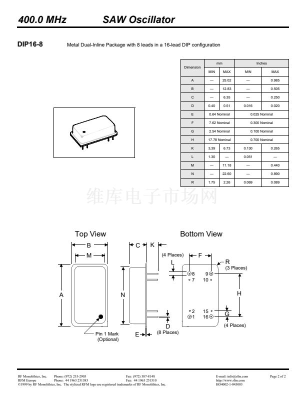
BLOCK DIAGRAM
V CC
RF OUTPUT
SAW Oscillator
Buffer Amplifier
ELECTRICAL CONNECTIONS
VCC 1
Case Ground 2
V tune
15 Case Ground
5.
6.
7.
Top
View
Case Ground 7
RF Output 8
10 Case Ground
9
V CC
RF Monolithics, Inc.
Phone: (972) 233-2903
Fax: (972) 387-8148
RFM Europe
Phone: 44 1963 251383
Fax: 44 1963 251510
漏1999 by RF Monolithics, Inc. The stylized RFM logo are registered trademarks of RF Monolithics, Inc.
E-mail: info@rfm.com
http://www.rfm.com
HO4002-1-043003
Page 1 of 2


 1
1
 2
2
