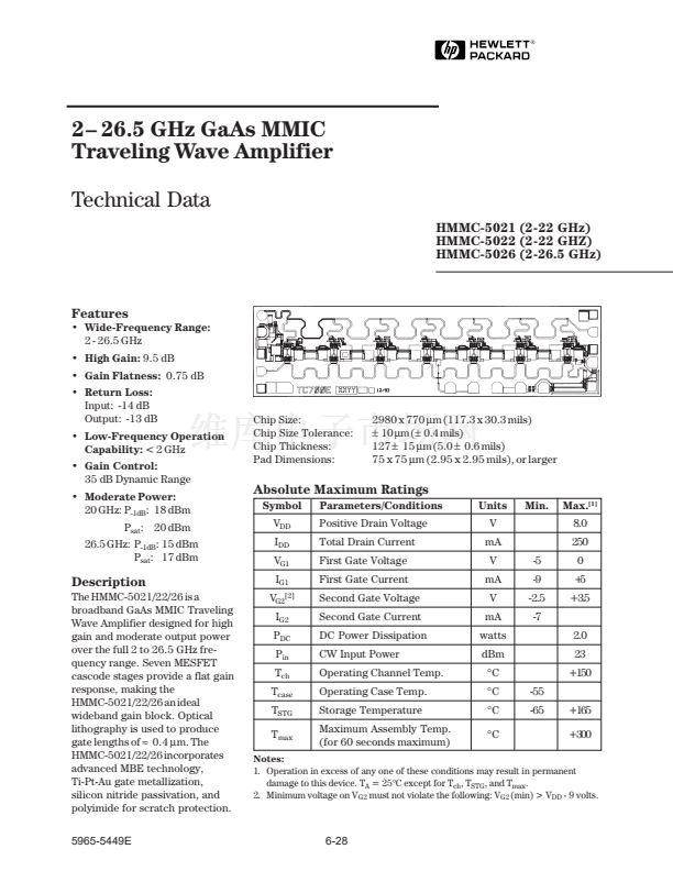
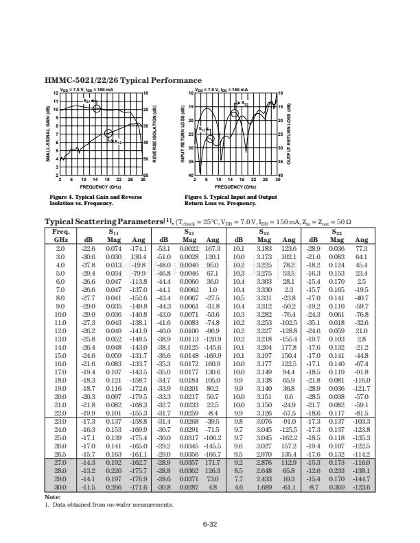
2鈥?26.5 GHz GaAs MMIC
Traveling Wave Amplifier
Technical Data
HMMC-5021 (2-22 GHz)
HMMC-5022 (2-22 GHZ)
HMMC-5026 (2-26.5 GHz)
Features
鈥?Wide-Frequency Range:
2 - 26.5 GHz
鈥?High Gain:
9.5 dB
鈥?Gain Flatness:
0.75 dB
鈥?Return Loss:
Input: -14 dB
Output: -13 dB
鈥?Low-Frequency Operation
Capability:
< 2 GHz
鈥?Gain Control:
35 dB Dynamic Range
鈥?Moderate Power:
20 GHz: P
-1dB
: 18 dBm
P
sat
: 20 dBm
26.5 GHz: P
-1dB
: 15 dBm
P
sat
: 17 dBm
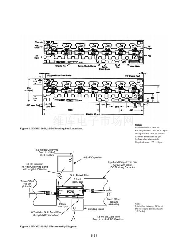
Chip Size:
Chip Size Tolerance:
Chip Thickness:
Pad Dimensions:
2980 x 770
碌m
(117.3 x 30.3 mils)
鹵
10
碌m
(鹵 0.4 mils)
127
鹵
15
碌m
(5.0
鹵
0.6 mils)
75 x 75
碌m
(2.95 x 2.95 mils), or larger
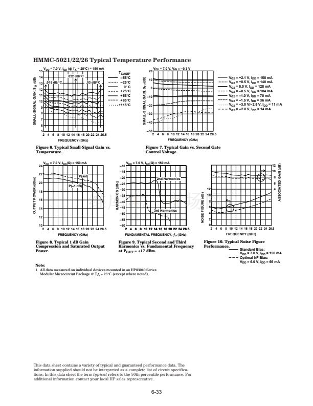
Absolute Maximum Ratings
Symbol
V
DD
I
DD
V
G1
I
G1
V
G2[2]
I
G2
P
DC
P
in
T
ch
T
case
T
STG
T
max
Parameters/Conditions
Positive Drain Voltage
Total Drain Current
First Gate Voltage
First Gate Current
Second Gate Voltage
Second Gate Current
DC Power Dissipation
CW Input Power
Operating Channel Temp.
Operating Case Temp.
Storage Temperature
Maximum Assembly Temp.
(for 60 seconds maximum)
Units
V
mA
V
mA
V
mA
watts
dBm
擄C
擄C
擄C
擄C
-55
-65
+165
+300
-5
-9
-2.5
-7
2.0
23
+150
Min.
Max.
[1]
8.0
250
0
+
5
+3.5
Description
The HMMC-5021/22/26 is a
broadband GaAs MMIC Traveling
Wave Amplifier designed for high
gain and moderate output power
over the full 2 to 26.5 GHz fre-
quency range. Seven MESFET
cascode stages provide a flat gain
response, making the
HMMC-5021/22/26 an ideal
wideband gain block. Optical
lithography is used to produce
gate lengths of
鈮?/div>
0.4
碌m.
The
HMMC-5021/22/26 incorporates
advanced MBE technology,
Ti-Pt-Au gate metallization,
silicon nitride passivation, and
polyimide for scratch protection.
5965-5449E
Notes:
1. Operation in excess of any one of these conditions may result in permanent
damage to this device. T
A
= 25擄C except for T
ch
, T
STG
, and T
max
.
2. Minimum voltage on V
G2
must not violate the following: V
G2
(min) > V
DD
- 9 volts.
6-28


 1
1
 2
2
 3
3
 4
4
 5
5
 6
6
