HM-6617/883
March 1997
2K x 8 CMOS PROM
Description
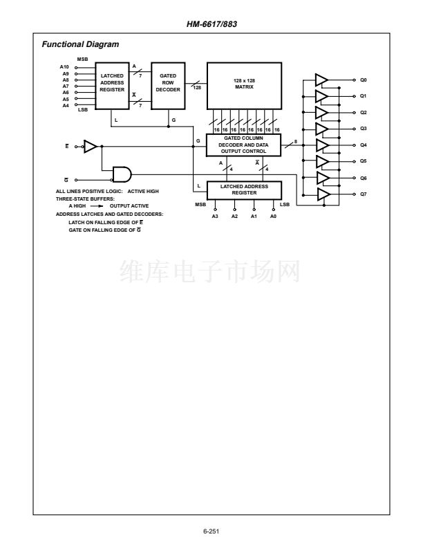
The HM-6617/883 is a 16,384-bit fuse link CMOS PROM in
a 2K word by 8-bit/word format with 鈥淭hree-State鈥?outputs.
This PROM is available in the standard 0.600 inch wide 24
pin SBDIP, the 0.300 inch wide slim SBDIP, and the JEDEC
standard 32 pad CLCC.
The HM-6617/883 utilizes a synchronous design technique.
This includes on-chip address latches and a separate output
enable control which makes this device ideal for applications
utilizing recent generation microprocessors. This design
technique, combined with the Intersil advanced self-aligned
silicon gate CMOS process technology offers ultra-low
standby current. Low ICCSB is ideal for battery applications
or other systems with low power requirements.
The Intersil NiCr fuse link technology is utilized on this and
other Intersil CMOS PROMs. This gives the user a PROM
with permanent, stable storage characteristics over the full
industrial and military temperature voltage ranges. NiCr fuse
technology combined with the low power characteristics of
CMOS provides an excellent alternative to standard bipolar
PROMs or NMOS EPROMs.
All bits are manufactured storing a logical 鈥?鈥?and can be
selectively programmed for a logical 鈥?鈥?at any bit location.
Features
鈥?This Circuit is Processed in Accordance to MIL-STD-
883 and is Fully Conformant Under the Provisions of
Paragraph 1.2.1.
鈥?Low Power Standby and Operating Power
- ICCSB . . . . . . . . . . . . . . . . . . . . . . . . . . . . . . . . .100碌A(chǔ)
- ICCOP . . . . . . . . . . . . . . . . . . . . . . . . . . 20mA at 1MHz
鈥?Fast Access Time. . . . . . . . . . . . . . . . . . . . . . . 90/120ns
鈥?Industry Standard Pinout
鈥?Single 5.0V Supply
鈥?CMOS/TTL Compatible Inputs
鈥?High Output Drive . . . . . . . . . . . . . . . . 12 LSTTL Loads
鈥?Synchronous Operation
鈥?On-Chip Address Latches
鈥?Separate Output Enable
鈥?Operating Temperature Range . . . . . . -55
o
C to +125
o
C
Ordering Information
PACKAGE
SBDIP
SLIM SBDIP
CLCC
TEMPERATURE RANGE
-55
o
C to +125
o
C
-55
o
C to +125
o
C
-55
o
C to +125
o
C
90ns
HM1-6617B/883
HM6-6617B/883
HM4-6617B/883
120ns
HM1-6617B/883
HM6-6617B/883
HM4-6617B/883
PACKAGE NO.
D24.6
D24.3
J32.A
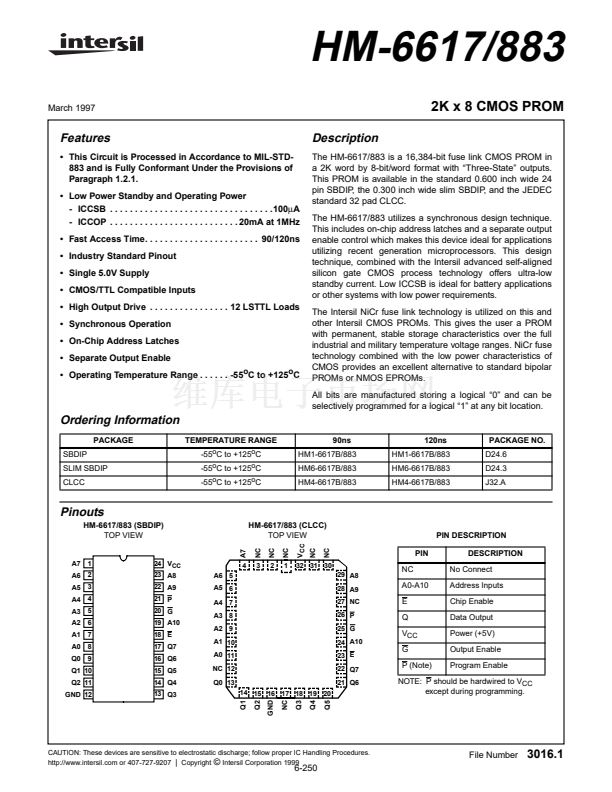
Pinouts
HM-6617/883 (SBDIP)
TOP VIEW
A7
HM-6617/883 (CLCC)
TOP VIEW
V
CC
NC
NC
NC
NC
NC
PIN DESCRIPTION
PIN
29 A8
28 A9
27 NC
26 P
25 G
24 A10
23 E
22 Q7
21 Q6
DESCRIPTION
No Connect
Address Inputs
Chip Enable
Data Output
Power (+5V)
Output Enable
Program Enable
A7
A6
A5
A4
A3
A2
A1
A0
Q0
1
2
3
4
5
6
7
8
9
24 V
CC
23 A8
22 A9
21 P
20 G
19 A10
18 E
17 Q7
16 Q6
15 Q5
14 Q4
13 Q3
4
A6 5
A5 6
A4 7
A3 8
A2 9
A1 10
A0 11
NC 12
Q0 13
3
2
1
32 31 30
NC
A0-A10
E
Q
V
CC
G
P (Note)
Q1 10
Q2 11
GND 12
14 15 16 17 18 19 20
Q1
Q2
Q3
Q4
GND
NC
Q5
NOTE: P should be hardwired to V
CC
except during programming.
CAUTION: These devices are sensitive to electrostatic discharge; follow proper IC Handling Procedures.
http://www.intersil.com or 407-727-9207
|
Copyright
漏
Intersil Corporation 1999
File Number
3016.1
6-250


 1
1
 2
2
 3
3
 4
4
 5
5
 6
6
 7
7
