HD74SSTV32852
24-bit to 48-bit Registered Buffer
with SSTL_2 Inputs and Outputs
ADE-205-687C (Z)
Rev.3
Nov. 2002
Description
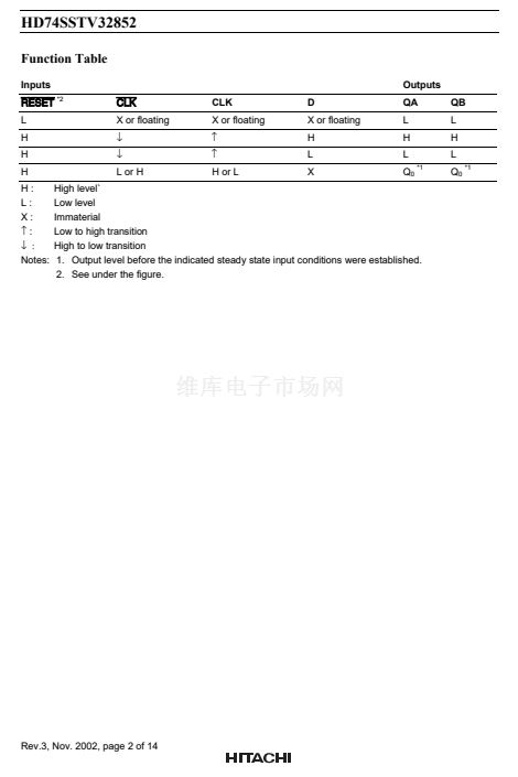
The HD74SSTV32852 is a 24-bit to 48-bit registered buffer designed for 2.3 V to 2.7 V Vcc operation and
LVCMOS reset (RESET) input / SSTL_2 data (D) inputs and CLK input.
Data flow from D to QA, QB is controlled by differential clock pins (CLK,
CLK)
and the
RESET.
Data is
triggered on the positive edge of the positive clock (CLK), and the negative clock (CLK) must be used to
maintain noise margins. When
RESET
is low, all registers are reset and all outputs are low.
To ensure defined outputs from the register before a stable clock has been supplied,
RESET
must be held in
the low state during power up.
Features
鈥?/div>
鈥?/div>
鈥?/div>
鈥?/div>
Supports LVCMOS reset (RESET) input / SSTL_2 data (D) inputs and CLK input
Differential SSTL_2 (Stub series terminated logic) CLK signal
Pinout optimizes DIMM PCB layout
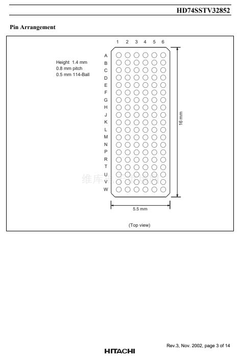
Ordering Information
Package Type
LFBGA-114pin
Package Code
BP-114
Package
Abbreviation
LB
Taping
Abbreviation (Quantity)
EL (1,000 pcs / Reel)
Part Name
HD74SSTV32852LBEL


 1
1
 2
2
 3
3
 4
4
 5
5
 6
6
 7
7
 8
8
 9
9
 10
10
 11
11
 12
12
 13
13
 14
14
